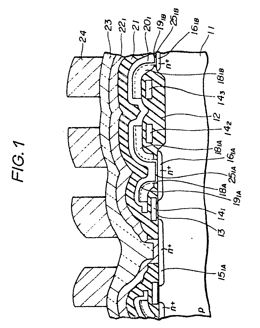
(57) A layer structure of a memory cell for a dynamic random access memory device includes
a semiconductor substrate (11), an insulation film (13, 17) formed on the semiconductor
substrate having a first window (18A, 27A) through which a surface of the semiconductor
substrate (11) is partially exposed, a first conductive film (181A, 181B, 281A, 281B) formed on the insulation film so as to surround the contact window (18A, 27A) and
form a second window (18A, 28A) above the first window (18A, 27A); a second conductive
film (251A, 251B, 351A, 351B) formed so as to be in contact with the first conductive film (181A, 181B, 281A, 281B), and the semiconductor substrate (11) through the first and second windows (18A,
27A, 28A) the first and second conductive films constructing a storage electrode of
a memory cell capacitor; a dielectric film (191A, 191B, 291A, 291B) formed so as to cover the storage electrode (181A, 181B, 281A, 281B, 251A, 251B, 351A, 351B); and a third conductive film (30₁) formed so as to cover the dielectric film (191A, 191B, 291A, 291B).
|
|
