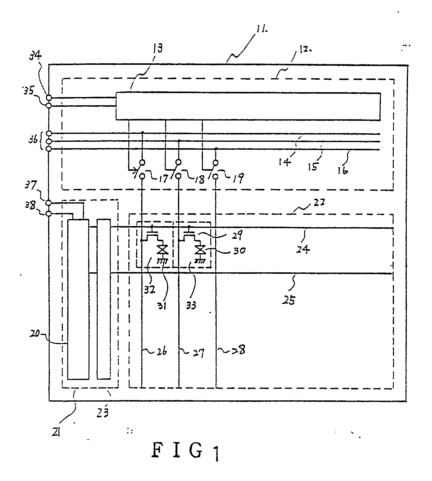
(57) An active matrix panel comprises a picture element matrix (22), which is mounted
on a transparent substrate (71, 86) and which includes a plurality of gate lines (24,
25), a plurality of source lines (26, 27, 28) and a plurality of picture elements
(32, 33). The active matrix panel further comprises a gate line drive circuit (21)
and a source line drive circuit (12). Each of the picture elements includes a thin
film transistor (29, 101) and, in addition, at least one of the gate line drive circuit
and the source line drive circuit comprises a plurality of thin film transistors (47
to 56; 58, 59; 99, 100) provided on the transparent substrate. For example, the at
least one of the gate line drive circuit and the source line drive circuit may comprise
complementary thin film transistors. The thin film transistors of the picture element
matrix have a similar cross sectional structure to at least certain of the thin film
transistors of the at least one of the gate line drive circuit and the source line
drive circuit.
|
|
