(19)
(11) EP 0 368 442 A3

(12) EUROPEAN PATENT APPLICATION

(88) Date of publication A3:
17.04.1991 Bulletin 1991/16

(43) Date of publication A2:
16.05.1990 Bulletin 1990/20

(21) Application number: 89307379.1

(22) Date of filing: 20.07.1989
(51) International Patent Classification (IPC)5G11B 7/24, G11B 7/26
(84) Designated Contracting States:
DE FR GB NL

(30) Priority: 08.11.1988 JP 281823/88
30.01.1989 JP 20999/89

(71) Applicant: PIONEER ELECTRONIC CORPORATION
Meguro-ku Tokyo 153 (JP)

(72) Inventors:
  • Iida, Tetsuya Pioneer Electronic Corporation
    Tsurugashima-machi Iruma-gun Saitama (JP)
  • Higuchi, Takanobu Pioneer Electronic Corporation
    Tsurugashima-machi Iruma-gun Saitama (JP)
  • Ogoshi, Kunizo Pioneer Electronic Corporation
    Tsurugashima-machi Iruma-gun Saitama (JP)
  • Yokozeki, Shinichi Pioneer Electronic Corporation
    Tsurugashima-machi Iruma-gun Saitama (JP)

(74) Representative: Brunner, Michael John et al
GILL JENNINGS & EVERY Broadgate House 7 Eldon Street
London EC2M 7LH
London EC2M 7LH (GB)


(56) References cited: : 


    (54) Optical information record carrier and the method of producing the same


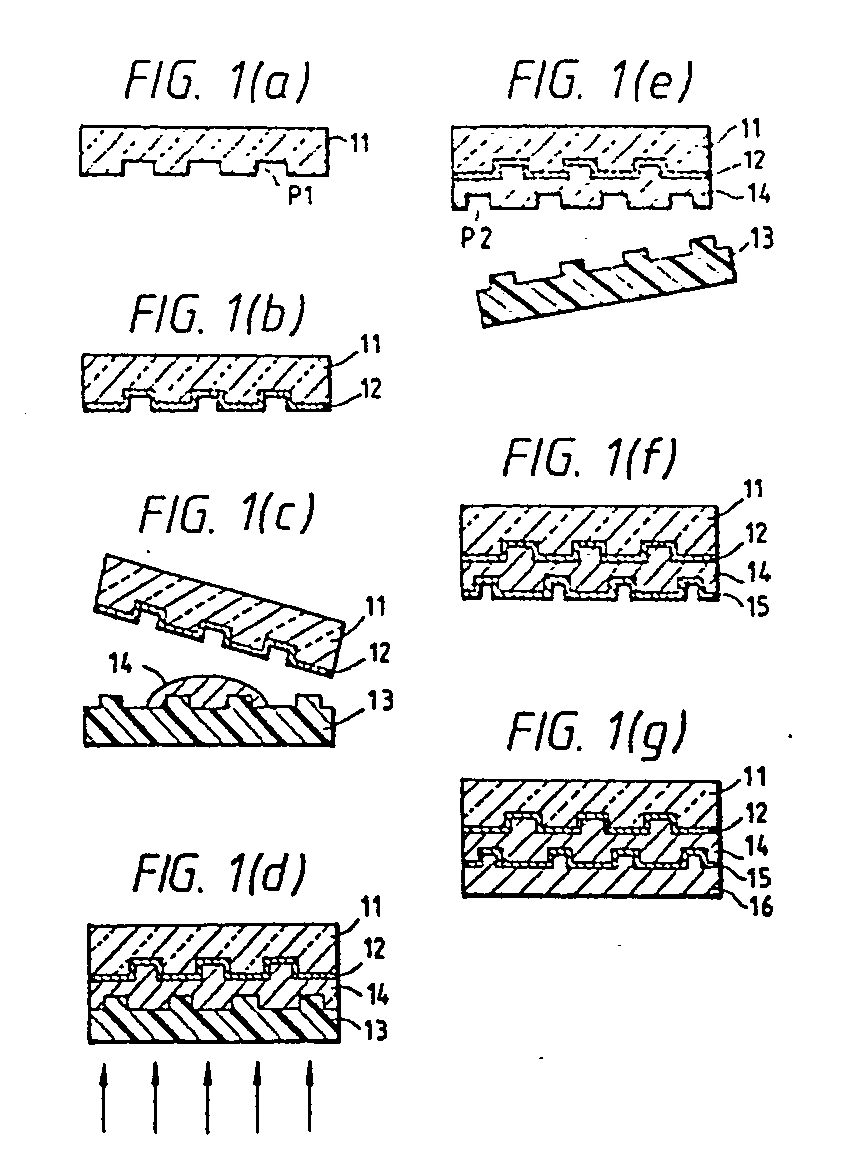
    (57) An optical information record carrier, in the form of an optical disk, has multiple reflective surfaces (12,15), each carrying separate information and each readable by an optical beam directed from the same side of the record carrier. The topmost reflective surface (12) reflects light of a first waveband and passes light of a second waveband. The next topmost reflective layer (15) reflects light within at least part of the second waveband. The record carrier may be formed by producing a first reflective layer (12) having a first pit pattern in the surface of a transparent substrate (11), pressing the first substrate/layer combination to a transparent stamper (13) having a second pit pattern, with a radiation hardening liquid resin (14) therebetween, irradiating the resin by applying radiation to the resin through the stamper, peeling off the stamper, applying a second reflective layer (15) to the hardened resin surface opposite the surface in contact with the first reflective layer, and applying a protective layer (16) to the second reflective layer.


    Search report