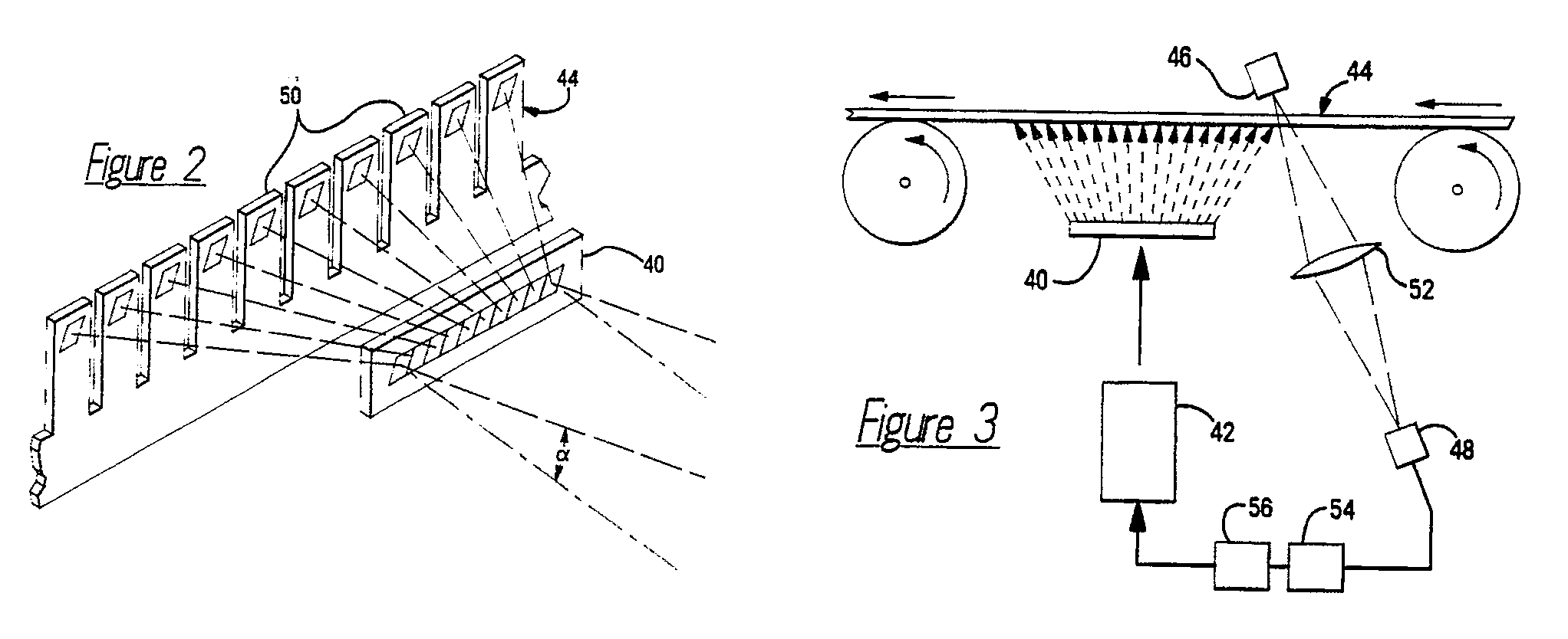
(57) In a method of splitting, imaging and focussing a pulsing laser beam, such as from
an excimer laser (42), onto a workpiece (44) to effect treatment to the surface thereof,
such as improving the surface for subsequent metal plating of such workpiece (44),
a preferred technique of laser assisted plating uses a system for laser ablating a
plurality of contact areas on electrical terminals (50), where said areas are covered
by an ablatable resist. The system comprises a carrier strip (44) having a plurality
of said electrical terminals (50) mounted thereon; a pulsed laser (42) for directing
radiation at said carrier strip (44); a hologram (40) mounted in the radiation path
between said laser (42) and said carrier strip (44) for splitting the radiation from
said laser (42) into a plurality of radiation beams directed towards said plurality
of contact areas; and means (48,52,54,56) for synchronising the movement of said
carrier strip (44) with the pulsing of said laser (42) so that a respective one of
said plurality of outgoing beams ablates said resist over a respective one of said
contact as said contact areas move past said hologram (40).
|
|
