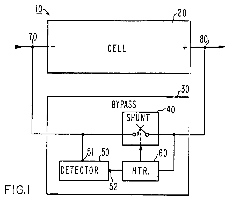
(57) A circuit bypass device (30) having terminals (70, 80) is connected to contacts (70,
80) of a cell (20) to provide a conductive path (40) in response to voltage excursion
therebetween. Device (30) includes: a conductive shunt (40), coupled to contacts (70,
80), that is movable from a normally non-conductive position to a conductive position
between terminals (70, 80); a detector (50), coupled to conductive shunt (40), for
sensing voltage excursion beyond specified limits between contacts (70, 80); and an
actuator (60) having a heat-to-recover shape memory metal alloy that is formed to
contract when detector (50) senses the voltage excursion, for moving conductive shunt
(40) from the non-conductive position to the conductive position. The formed alloy
is preferably spring-shape which contracts translationally and torsionally.
|
|
