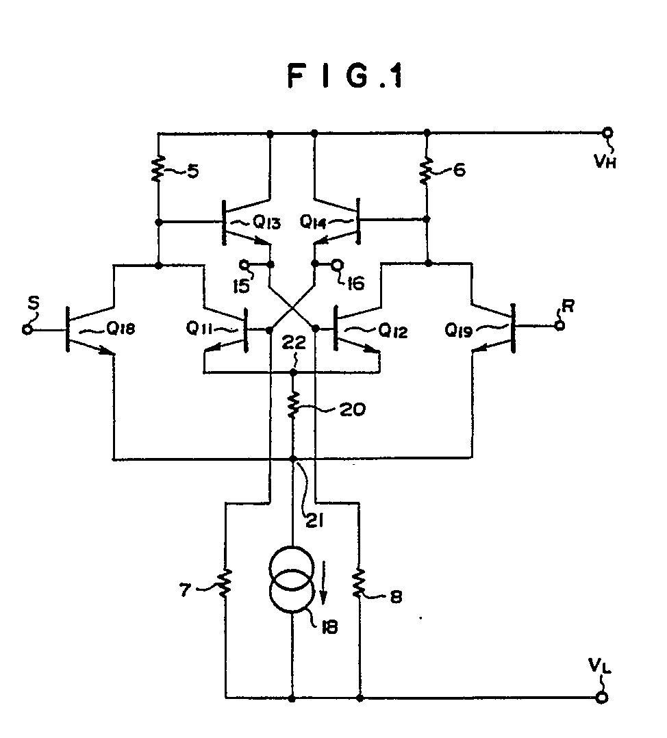
(57) A Flip-Flop circuit, of a current-pass switching type logical circuit, of the invention
comprises a pair of data holding transistors (Q₁₁,Q₁₂), the emitters thereof being
tied together at a first junction point (22) and being led to a constant-current source
(18); and a set signal input transistor (Q₁₈) and a reset signal input transistor
(Q₁₉), the emitters thereof being tied together at a second junction point (21) and
being led to the constant-current source. There is provided a single level-shifting
resistor (20) between the first junction point (22) and the second junction point
(21) for preventing interference or concurrence between the high level of a set signal
or a reset signal and the high level of the internal data held by the data holding
transistors (Q₁₁,Q₁₂). The circuit is suitable to be fabricated in a semiconductor
integrated circuit device of high packing density. The working range of power supply
voltages for the circuit is wide because the level shift voltage developed across
the level-shifting resistor is not influenced by the variation of the power supply
voltage.
|
|
