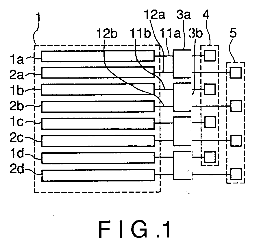
(57) A semiconductor memory device a memory cell array (1), a data register unit (4, 5),
and a data transfer gate unit (3a, 3b). The memory cell array (1) includes first memory
cell arrays (1a, 1b,...) and second memory cell arrays (2a, 2b,...) alternately disposed.
The data register unit (4, 5) includes first data registers (4a, 4b,...) and second
data registers (5a, 5b,...) alternately disposed. Each of a plurality of data transfer
gates of the data transfer gate unit (3a, 3b) includes a gate (25) for connecting
each of the first memory cell arrays (1a, 1b,...) to each of the first data registers
(4a, 4b,...), and a gate (27) for connecting each of the second memory cell arrays
(2a, 2b,...) to each of the second registers (5a, 5b,...), and further includes a
gate (26) for connecting each of the first memory cell arrays (1a, 1b,...) to each
of the second data registers (5a, 5b,...), and a gate (28) for connecting each of
the second memory cell arrays (2a, 2b,...) to each of the first data registers (4a,
4b,...).
|
|
