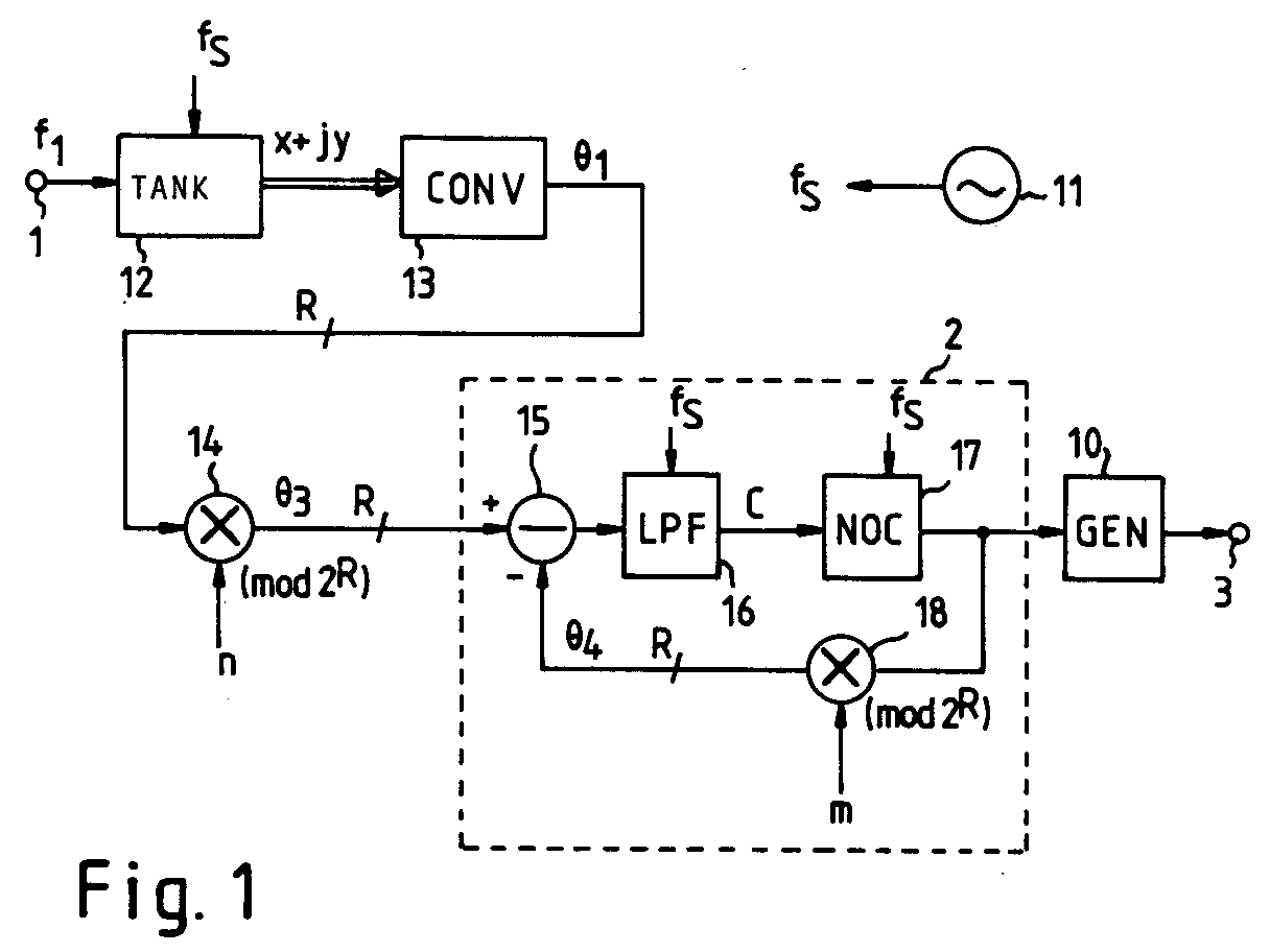
(57) A first clock signal of f1 in frequency is converted into a second clock signal having
a frequency of f2 =

f1. The first clock signal is converted by a tank circuit (12) and a converter (13)
into an R-bit first phase signal (ϑ1) indicating the phase of the first clock signal.
The first phase signal is multiplied by n (mod 2R) by a multiplier into a second phase signal (ϑ3). The second phase signal is supplied
to a digital phase-locked loop (PIL) (3) consisting of a subtractor (15), a low-pass
filter (LPF) (16), a numerically controlled oscillator (NCO) (17) and a multiplier
(18). The multiplier in the digital PIL (3) multiplies by m (mod 2R) a third phase signal, indicating the phase of a second clock signal which is the
output of the NCO (17), to generate a fourth phase signal. The subtractor (15) generates
a signal representing the phase error between the second and fourth phase signals.
This phase error signal is filtered by the LPF (16) to control the oscillating phase
of the NCO (17). A clock generating circuit generates, on the basic of the third phase,
signal, the second clock signal.
|
|
