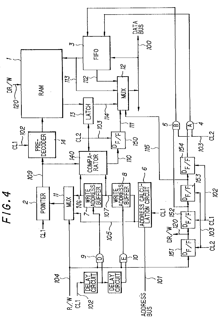
(57) A FIFO type buffer circuit (3) is positioned to hold write-data between a random
access memory (1) and a system data bus (100). A shift circuit (7,8) is positioned
between an address calculation circuit (6) and a pointer circuit (2). The system data
bus is connected to an output of the FIFO buffer circuit or to a read-data circuit
of the random access memory, dependent on the operation mode, namely writing or reading
mode, and the pointer circuit is connected to the address calculation circuit or to
the shift circuit dependent on the operation mode. Accordingly, pipe line control
is realized, even if the data transfer and the memory processing are reversed in order
between the writing and reading modes.
|
|
