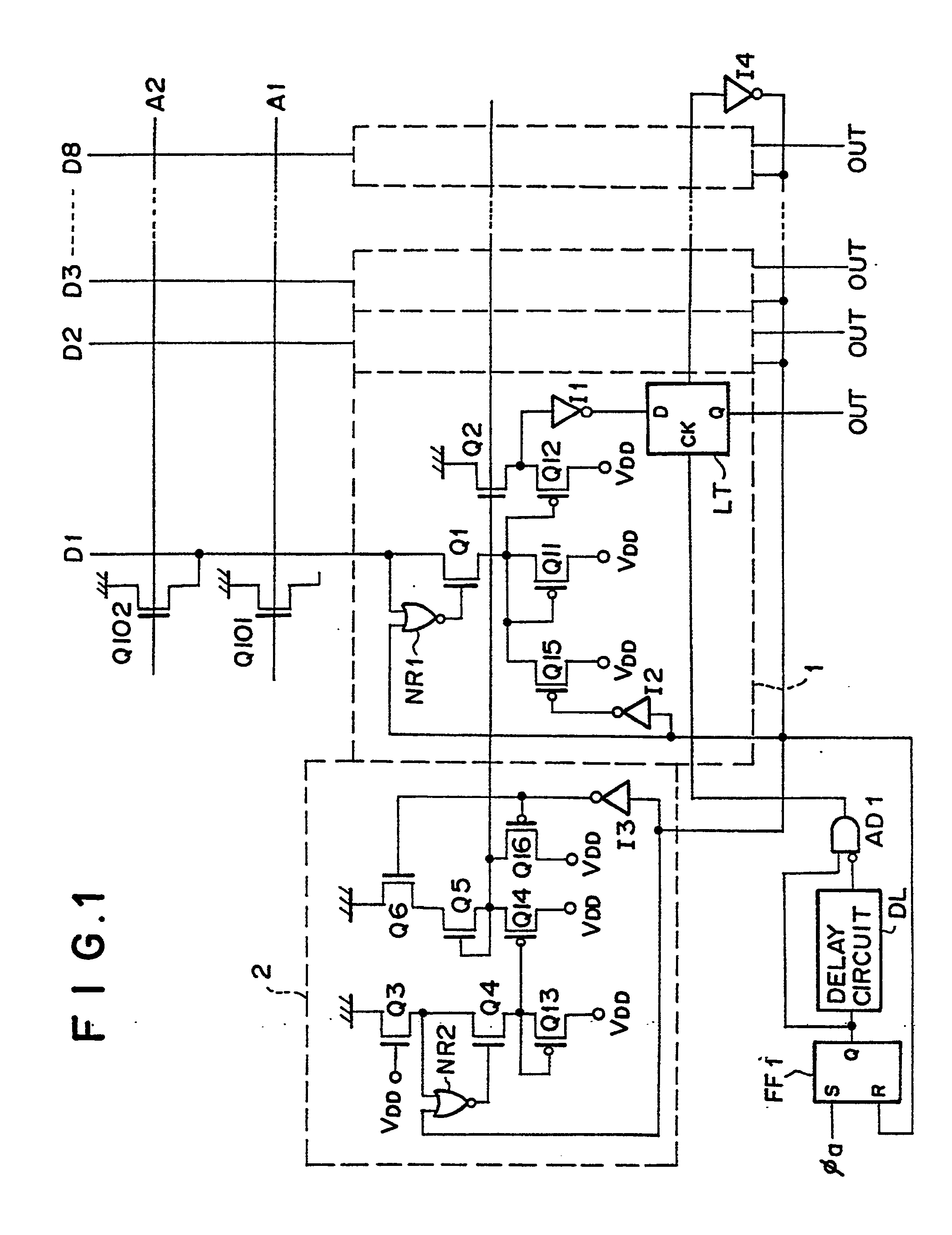
(57) A memory device of the invention has memory cells (Q101,Q102) each of which is addressed
according to a timing signal (øa), current sense amplifiers (1) each of which determines
whether a current flows in the addressed memory cell or not and reads out data stored
in such memory cell, a circuit (FD1,DL,AD1; DL,AD2,FF3) which generates a control
signal to become active at a timing when the memory cell is addressed and to become
inactive after read-out of the stored data is completed, and a circuit (I4,I2,NR1;
I4,FF2,NR1) which cuts-off based on the control signal a path for a steady-state current
flowing in the current sense amplifier.
|
|
