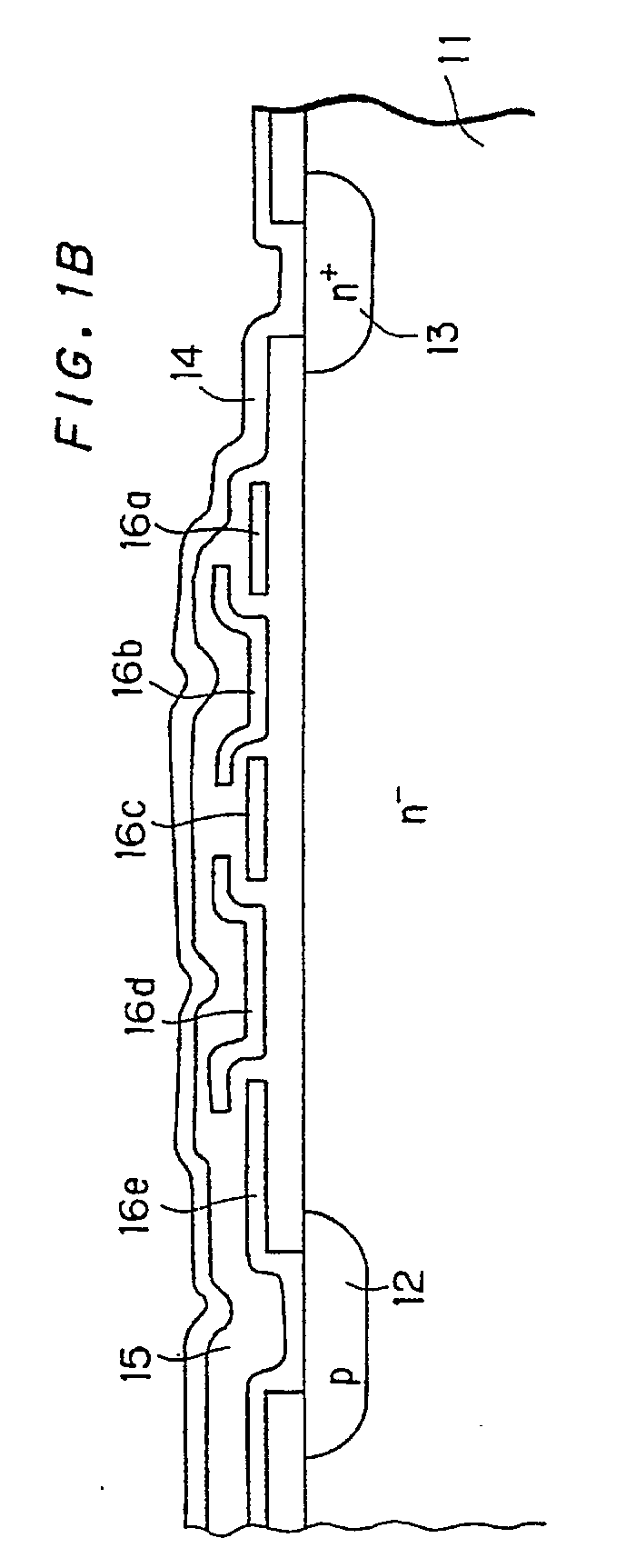
(57) Conductive plates (16a - 16e), or floating semiconductor regions (17a - 17d), or
conductive plates (16a, 16c, 16e) and floating semiconductor regions (17a, 17d) are
disposed in alignment so that a coupling capacitance between the conductive plates
and/or the floating semiconductor regions which are adjacent to each other descrease
as a distance from a first or second semiconductor region (12, 13) increases. Therefore,
the respective potentials at the conductive plates or the floating semiconductor regions
can be varied linearly (or at equal potential differences), and corresponding potential
distribution can be achieved on the surface of a semiconductor substrate (11). As
a result, electric field concentration on the surface of the semiconductor substrate
(11) just under a high potential conductive layer (14) can be prevented effectively
even by the use of an insulating layer (15) with a common thickness.
|
|
