(19)
(11) EP 0 528 291 A3

(12) EUROPEAN PATENT APPLICATION

(88) Date of publication A3:
11.05.1994 Bulletin 1994/19

(43) Date of publication A2:
24.02.1993 Bulletin 1993/08

(21) Application number: 92113478.9

(22) Date of filing: 07.08.1992
(51) International Patent Classification (IPC)5H01L 23/433, H01L 23/367
(84) Designated Contracting States:
CH DE FR GB IT LI NL

(30) Priority: 08.08.1991 JP 199554/91
08.08.1991 JP 199558/91
08.08.1991 JP 199561/91

(71) Applicant: SUMITOMO ELECTRIC INDUSTRIES, LIMITED
Osaka 541 (JP)

(72) Inventor:
  • Nishiguchi, Masanori, c/o Yokohama Works of
    Yokohama-shi, Kanagawa (JP)

(74) Representative: Lehn, Werner, Dipl.-Ing. et al
Hoffmann, Eitle & Partner, Patentanwälte, Postfach 81 04 20
81904 München
81904 München (DE)


(56) References cited: : 


    (54) Semiconductor chip module and method for manufacturing the same


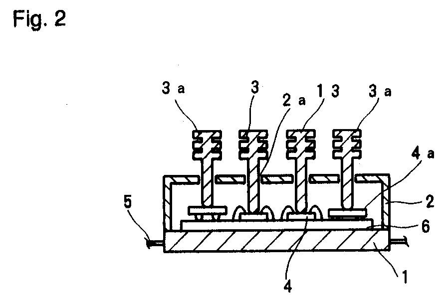
    (57) The semiconductor chip module comprises a substrate (6) on which a wiring portion is formed, a semiconductor chip (4) mounted so as to face a circuit side up to the wiring portion, a heat sink (3, 3a, 13) with one end thereof contacted to the central portion of an upper surface of the semiconductor chip (4, 4a); and a cap (2) which has an opening (2a) for exposing the other end of the heat sink (3, 3a, 13) to the outside thereof, the cap (2) enclosing all of the semiconductor chips (4, 4a). Accordingly, the heat generated from the semiconductor chips (4, 4a) can be dissipated through the heat sink (3, 3a, 13) to the outside. It results in providing a semiconductor chip module without inconvenience for operation with high speed.


    Search report