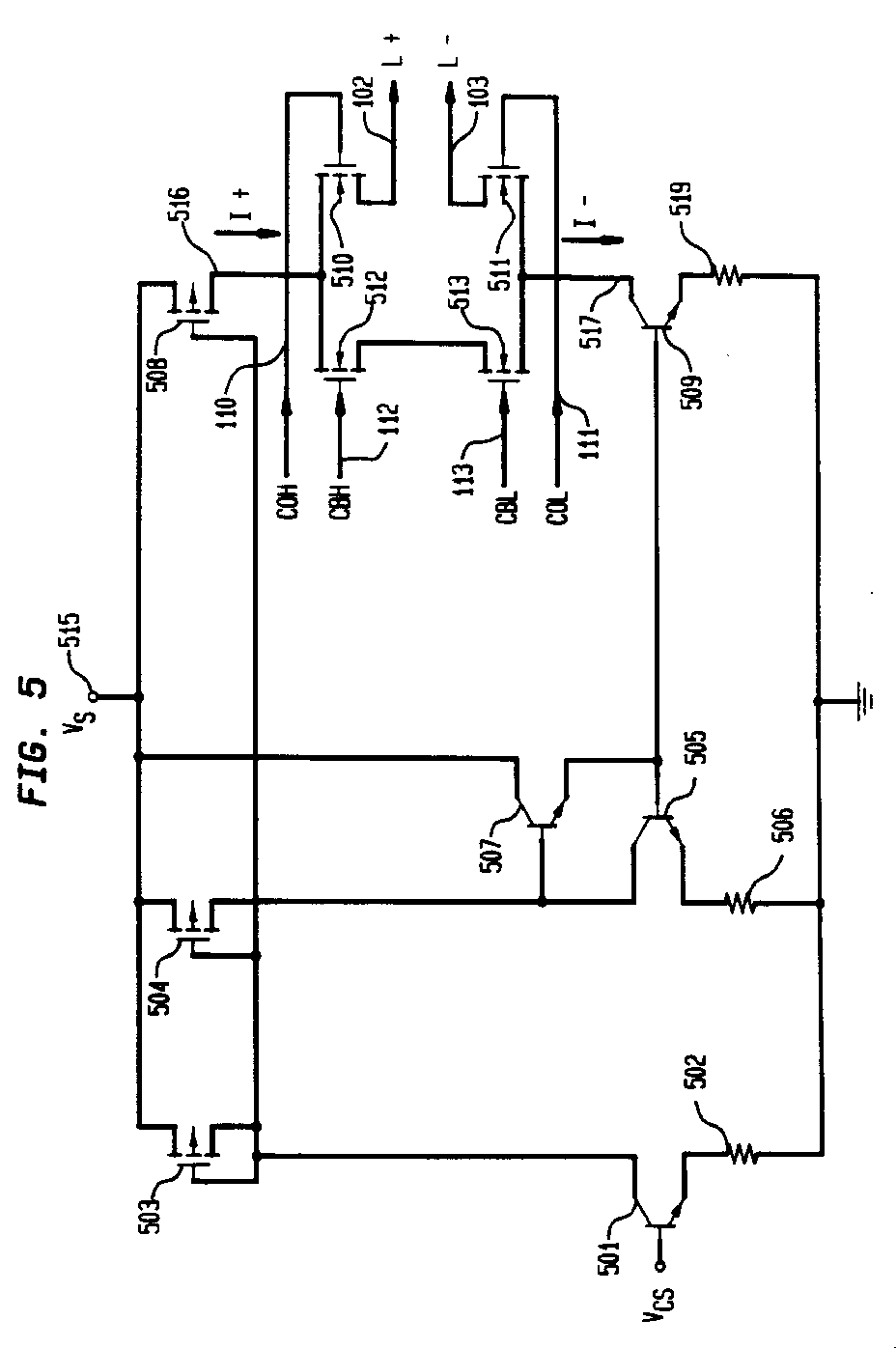
(57) A current mode bus driver couples input digital signals to a bus (L+,L-) which is
normally biased with a voltage difference representing one binary type. The current
mode bus driver responds to input digital signals of the other binary type by connecting
a current source (503,504,508) to one lead (L+) of the bus and a current sink (505,507,509)
to the other lead (L-) of the bus, thereby driving the bus to a voltage difference
which represents the other binary type. In response to input digital signals of the
first-mentioned binary type, the bus driver isolates the current source and current
sink from the bus and connects the current source directly to the current sink. The
selective switching is performed by n-channel MOSFETs (510-513) which are driven by
the input digital signals (CBH,CBL,COH,COL) through unique buffer driver circuits
employing a CMOS inverter, an n-channel MOSFET and an NPN transistor. A combination
of MOSFETs and NPN transistors provide a current source (503,504,508) and sink (505,507,509)
that permit operation of the bus at very low voltage levels.
|
|
