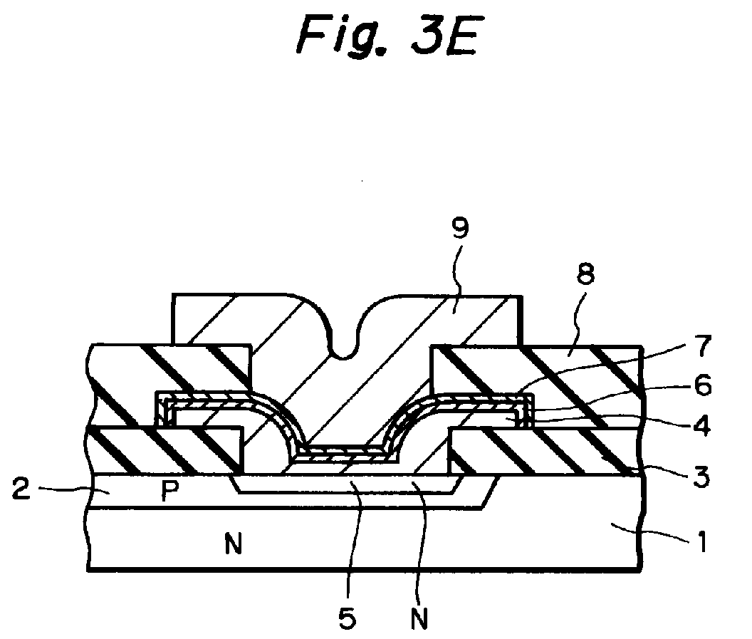
(57) In a semiconductor device including a semiconductor substrate (1), an impurity doped
region (5) formed in the semiconductor substrate, an insulating layer (3) formed on
the semiconductor substrate and having an opening leading to the impurity doped region,
a polycrystalline silicon layer (4, 4', 4'') formed on the insulating layer and the
impurity doped region, and a metal silicide layer (6) formed on the polycrystalline
silicon layer, a transverse thickness of the polycrystalline silicon layer at a sidewall
of the insulating layer is larger than a longitudinal thickness of the polycrystalline
silicon layer at a bottom of the opening and at a surface of the insulating layer.
|
|
