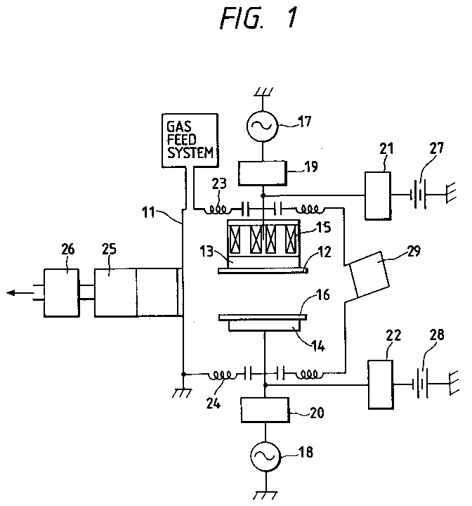
(57) A method for forming a deposited film by a bias sputtering process comprises the
steps of generating plasma between a target electrode holding a target material (18)
provided in a vacuum container (11) and a substate electrode (14) holding a substrate
(16) for forming deposited film, provided opposingly to the target electrode, by the
use of a high-frequency energy to cause the target material to undergo sputtering,
and applying a bias voltage to at least one of the target electrode (13) and the substate
electrode (14) to form a deposited film comprised of atoms having deposited by sputtering
on the substrate, wherein;
a mixed-gas environment comprising a mixture of an inert gas and a hydrogen gas
is formed in the vacuum container, and the target material (12) is subjected to sputtering
while controlling H2O gas, CO gas and CO2 gas in the mixed-gas environment to have a partial pressure of 1.0 × 10⁻⁸ Torr or less each, to form an epitaxial film on the substrate (16) while maintaining
a substrate temperature in the range of from 400°C to 700°C.
|
|
