(19)
(11) EP 0 676 810 A3

(12) EUROPEAN PATENT APPLICATION

(88) Date of publication A3:
11.12.1996 Bulletin 1996/50

(43) Date of publication A2:
11.10.1995 Bulletin 1995/41

(21) Application number: 95104914.7

(22) Date of filing: 03.04.1995
(51) International Patent Classification (IPC)6H01L 27/092, H01L 29/78
(84) Designated Contracting States:
DE FR GB

(30) Priority: 04.04.1994 US 223394

(71) Applicant: MOTOROLA, INC.
Schaumburg, IL 60196 (US)

(72) Inventors:
  • Kaneshiro, Michael H.
    Phoenix, Arizona 85044 (US)
  • Dow, Diann
    Chandler, Arizona 85224 (US)

(74) Representative: Hudson, Peter David et al
Motorola European Intellectual Property Midpoint Alencon Link
Basingstoke, Hampshire RG21 7PL
Basingstoke, Hampshire RG21 7PL (GB)


(54) Insulated gate field effect transistor and method of fabricating


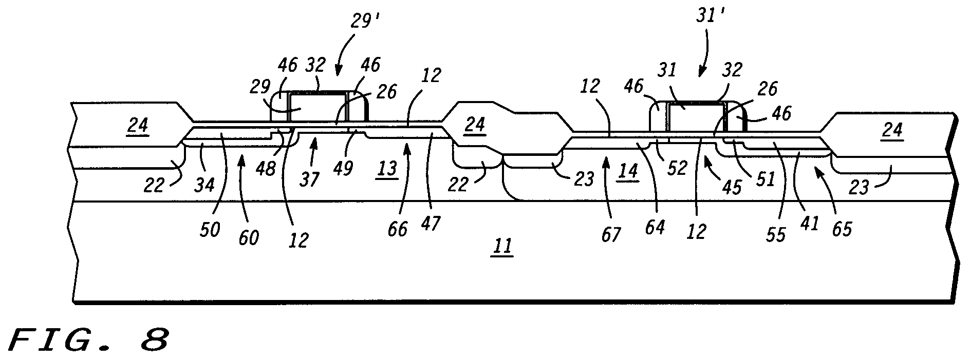
(57) Insulated gate field effect transistors (10, 70) having independent process steps for setting lateral and vertical dopant profiles for source and drain regions. In a unilateral transistor (10), portions (48, 50, 51, 55) of the source region are contained within a halo region (34, 41) whereas portions (49, 47, 52, 64) of the drain region are not contained within a halo region. The source region (60, 65) has a first portion (48, 51) for setting a channel length and a second portion (50, 55) for setting a breakdown voltage and a source/drain capacitance. The second portion (50, 55) extends further into the halo region than the first portion (48, 51). In a bilateral transistor (70), portions (84, 89, 80, 91) of the drain region (72, 77) are contained within halo region (75, 79).


Search report