|
(11) | EP 0 702 204 B1 |

| (12) | EUROPEAN PATENT SPECIFICATION |
|
|
| (54) |
A method of evaluating silicon wafers Verfahren zur Auswertung von Siliziumscheiben Procédé d'évaluation de plaquettes de silicium |
|
|
|||||||||||||||||||||||||||||||
| Note: Within nine months from the publication of the mention of the grant of the European patent, any person may give notice to the European Patent Office of opposition to the European patent granted. Notice of opposition shall be filed in a written reasoned statement. It shall not be deemed to have been filed until the opposition fee has been paid. (Art. 99(1) European Patent Convention). |
Background of the Invention
1. Field of the Invention
[0001] This invention relates in general to a method of evaluating silicon wafers and more particularly to a method of evaluating the crystal quality near surface of silicon wafers by means of a microroughness analysis.
2. The Prior Art
[0002] A silicon wafer used for manufacturing semiconductor integrated circuits has a device(s) formed on and near surface thereof. The flatness of the surface, an active area of the device(s) is formed thereon, of the silicon wafer is crucial in both macroscopic and microscopic levels. As unevenness at the atomic level, called microroughness, is believed to be reflected by the crystal quality, this microroughness has been evaluated using various techniques.
[0003] The microroughness of a silicon wafer surface gets worse after the treatment with a cleaning solution composed of aqueous solution of ammonium hydroxide (NH4OH) and hydrogen peroxide (H2O2). Such change of the microroughness after the treatment with a cleaning solution having a relatively weak etching effect on silicon wafers is believed to be reflected by the crystal quality.
[0004] However, this etching effect of the cleaning solution is so weak that a technique to detect the microroughness with high sensitivity is required. Moreover, a technique with capability to measure the order of atomic level is required.
[0005] An atomic force microscope (hereafter referred to as "AFM") and a scanning tunnelling microscope (hereafter referred to as "STM") are used in techniques for the measurement of the microroughness of silicon wafers in the order of atomic level. An AFM detects the microscopic forces between atoms and a probe, typically van der Waals forces, and detects changes in such forces due to minute differences in the distances between atoms and the probe to determine the surface unevenness.
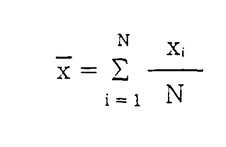
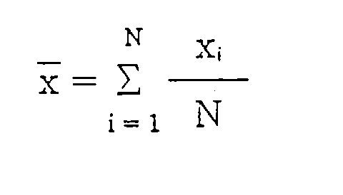
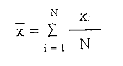
[0006] Since an AFM is capable of very accurately measuring unevenness without destruction of the surface of the specimen, it is ideal for measuring the microroughness. The microroughness obtained by AFM is usually represented by RMS (root mean square), P-V (peak to valley) and so on. Assuming xi (i = 1, 2, ... , N) to be the height of one of N measurement points from the reference plane, RMS is expressed by the following equation:
Where
denotes:
[0007] P-V is expressed by the following equation:
Where [xi]max is the maximum of xi and [xi]min is the minimum of xi.
[0008] As a prior art for the microroughness change evaluation of silicon wafers after the treatment with a cleaning solution having a composition of NH4OH/H2O2/H2O = 1:1:5, T.Ohmi et al. reported the relationship between the microroughness and the crystal quality of various samples including Czochralski grown crystals, float zoned crystals and epitaxial grown crystals using average roughness (Ra).
[0009] Here, Ra is a microroughness evaluation similar to RMS, as shown in the following equation:
Where
denotes:
[0010] The evaluation method described above takes measurements in a scanning area of a prescribed size at several points. RMS value is shown to change differently depending on the types of silicon crystals when the microroughness measurements are carried out on a silicon wafer using different sizes of scanning area.
[0011] Figure 3 shows the relationship between the size of the scanning area (horizontal axis) and RMS (vertical axis) in the evaluation method described above. In this figure, the samples represented by circles have a haze level of 7 (BIT) without a heat treatment, the samples represented by squares have a haze level of 16 (BIT) with 20 minutes of a heat treatment at 1000°C, and the samples represented by triangles have a haze level of 107 (BIT) with several hours of a heat treatment at 1100°C. "Haze level" is an indicator of the microroughness obtained by an optical method, and a larger haze level values indicates more rough surface. As shown in the figure, the RMS value changes depending on the size of the scanning area and a good correlation with the haze level cannot be obtained.
[0012] The evaluation method described above has to be a microroughness evaluation based on RMS or Ra using a certain fixed size of the scanning area. However, such a RMS microroughness evaluation with a fixed size of the scanning area is not an appropriate evaluation of the crystal quality because it is not comprehensive. That is, because the scanning area of the AFM measurement is very small, it is difficult to grasp the silicon surface configuration with a calculation method such as RMS.
[0013] On the other hand, the microroughness of a silicon wafer surface affects the dielectric breakdown properties of an oxide layer. However, the evaluation of dielectric breakdown properties with a fabricating MOS structure on a silicon wafer surface requires complicated and time consuming process such as oxidation or formation of electrodes.
[0014] The document MICROELECTRONIC PROCESSES, SENSORS, AND CONTROLS, MONTEREY, CA, USA, 27-29 SEPT. 1993, vol. 2091, ISSN 0277-786X, PROCEEDINGS OF THE SPIE - THE INTERNATIONAL SOCIETY FOR OPTICAL ENGINEERING, 1994, USA, pages 51-62, XP002004209 GRANT J M ET AL: "Characterization of rapid thermally grown dielectrics by surface charge analysis and atomic force microscopy" and the document 1993 INTERNATIONAL CONFERENCE ON SOLID STATE DEVICES AND MATERIALS (SSDM '93), CHIBA, JAPAN, 29 AUG.-1 SEPT. 1993, vol. 33, no. 1 B, ISSN 0021-4922, JAPANESE JOURNAL OF APPLIED PHYSICS, PART 1 (REGULAR PAPERS & SHORT NOTES), JAN. 1994, JAPAN, pages 383-387, XP002004379 YOSHINOBU T ET AL: "Scaling analysis of SiO/sub 2//Si interface roughness by atomic force microscopy" both propose different scale-independent correlation functions to evaluate the roughness of surfaces.
Brief Summary of the Invention
[0015] The object of the present invention is to solve the problems described above and its objective is to detect with high sensitivity changes in the surface configuration of a silicon wafer and thus to provide a method of evaluating the crystal quality of silicon wafers.
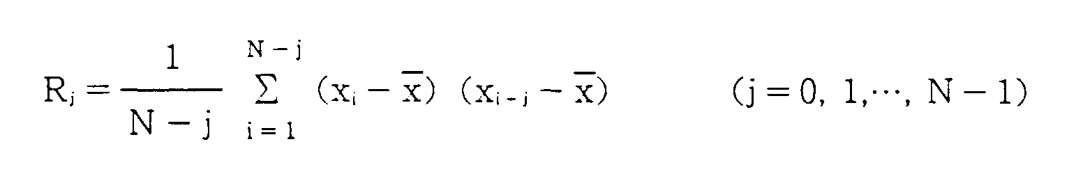
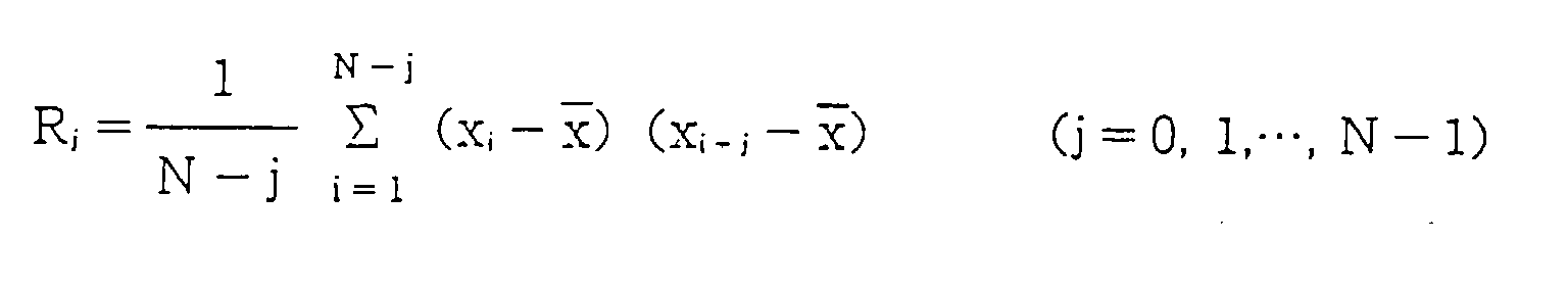
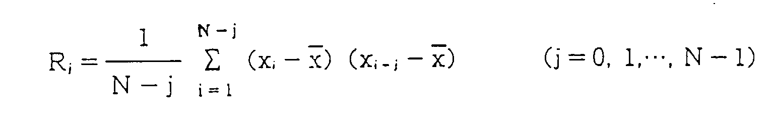
[0016] The present invention evaluates the crystal quality of silicon wafers by measuring the height xi (i = 1, 2, ..., N) of a plurality of measuring points on a silicon wafer from a reference plane by means of an AFM, determining the autocorrelation function Rj represented by:
wherein
denotes:
selecting an arbitrary number of autocorrelation function Rj with large value, and analyzing the microroughness on said silicon wafer based on the distances between the point Rj=0 and said selected points Rj's with large value except for Rj=0. " An arbitrary number" mentioned above is not limited in particular, but a number which is 2 or more and allows processing with a computer would be practical.
[0017] Said silicon wafers should preferably be treated with a cleaning solution composed of ammonium hydroxide (NH4OH), hydrogen peroxide (H2O2) and water before said measurement with the AFM is conducted. The ratio of NH4OH : H2O2 : H2O in said cleaning solution should preferably be 1 : 1 : 5.
[0018] The present invention is focused on the periodicity of the microroughness on a silicon wafer surface revealed by the AFM measurement, uses the autocorrelation function to observe the surface configuration between each silicon crystal and thus evaluates the crystal quality.
[0019] The periodicity of the microroughness on silicon wafer surface has not been studied at all. However, the inventors discovered that the microroughness has a periodic nature. Consequently, although the microroughness has been believed to be random unevenness, it has become possible, by analyzing the correlation between each unevenness using the autocorrelation function, to evaluate the microroughness in the atomic level measured by an AFM as a periodic function.
Brief Description of the Drawings
[0020] Figure 1 is a graph showing the periods of the microroughness and relative power for wafers with the low pulling speed.
[0021] Figure 2 is a graph showing the periods of the microroughness and relative power for wafers with the high pulling speed.
[0022] Figure 3 is a graph showing the relationship between the size of the scanning area and RMS in the evaluation of the microroughness of silicon wafers using RMS of the AFM measurements.
Detailed Description
[0023] Examples of the present invention are described below. CZ silicon single crystal wafers grown by different crystal pulling speeds (wafers grown by a low pulling speed of 0.4 mm/min and wafers grown by a high pulling speed of 1.1 mm/min) were dipped in a cleaning solution (NH4OH : H2O2 : H2O = 1 : 1: 5) for 0, 30, 60 and 90 minutes.
[0024] An AFM was used to measure the height xi (i = 1, 2, ..., N) of a plurality of measuring points on each silicon wafer from a reference plane, and the autocorrelation function Rj represented by the equation below was obtained:
Where
denotes:
[0025] 5 points with large value except for Rj=0 were selected to obtain their relative powers from among the autocorrelation function Rj's. For each of the selected 5 points, the correlation distance was calculated as a distance between the point Rj=0 and the selected Rj point with large value. Finally, the relationship between the correlation distance and the relative power for the wafers grown by the low pulling speed (0.4 mm/min) is shown in Figure 1 and such relationship for the wafers grown by the high pulling speed (1.1 mm/min) is shown in Figure 2.
[0026] The horizontal axis of Figure 1 and Figure 2 represents the correlation distance, i.e. the period of the microroughness, and the vertical axis represents the value of the autocorrelation function Rj, i.e. the strength of correlation for that period. A stronger correlation indicates that the microroughness at specific period gets worse more greatly. As shown in Figure 2, the microroughness of its correlation distance being 400 nm or less gets worse much more rapidly in the case of the wafers grown by high pulling speed. On the contrary, as shown in Figure 1, the microroughness of any typical period show no aggravation in the case of the wafers grown by low pulling speed. This is believed to indicate that the wafers grown by the low pulling speed are harder to be etched upon by said cleaning solution and have a a relatively good crystal quality.
[0027] As shown in the aforementioned results, there is a close relationship between the crystal manufacturing conditions of wafers and aggravation of the microroughness, and this evaluation method can detect the crystal quality near the surface of the silicon wafer with high sensitivity and thus replace the conventional evaluation method measuring dielectric breakdown voltage of an oxide layer which is complicated and time consuming.
[0028] As described thus far, the present invention, by taking the periodicity of the microroughness on a silicon wafer into account, can detect with high sensitivity changes in the surface configuration of the silicon wafer which could not be detected with conventional methods and makes it possible to evaluate the crystal quality near the surface of the silicon wafer. The present invention also allows acquisition of information about periods of the microroughness developed due to a treatment using a cleaning solution comprising a mixed aqueous solution of ammonium hydroxide and hydrogen peroxide. The evaluation can be done in a relatively short period of time without complicated procedures such as are required in the evaluation of the dielectric breakdown voltage of an oxide layer.
1. A method of evaluating silicon wafers which evaluates the crystal quality of silicon
wafers by measuring the height xi (i = 1, 2, ..., N) of a plurality of measuring points on the principal plane of a
silicon wafer from a reference plane by means of an atomic force microscope (hereafter
referred to as "AFM"), determining the autocorrelation function Rj represented by
wherein

denotes:
selecting an arbitrary number of autocorrelation function Rj with large value from said autocorrelation function Rj, and analyzing the microroughness on said silicon wafer based on the distances between the point Rj=0 and said selected points Rj's with large value except for Rj=0.
wherein
denotes:
selecting an arbitrary number of autocorrelation function Rj with large value from said autocorrelation function Rj, and analyzing the microroughness on said silicon wafer based on the distances between the point Rj=0 and said selected points Rj's with large value except for Rj=0.
2. A method of evaluating silicon wafers as described in Claim 1 wherein said silicon
wafers are treated with a cleaning solution composed of ammonium hydroxide (NH4OH), hydrogen peroxide (H2O2) and water before said measurement with the AFM is conducted.
3. A method of evaluating silicon wafers as described in Claim 2 wherein the ratio of
NH4OH : H2O2 : H2O in said cleaning solution is 1 : 1 : 5.
1. Verfahren zum Bewerten von Siliciumwafern, bei dem die Kristallqualität von Siliciumwafern
bewertet wird durch Messen der Höhe xi (i = 1, 2, ..., N) einer Vielzahl von Meßpunkten auf der Hauptebene eines Siliciumwafers
von einer Referenzebene aus mittels eines Atomkraftmikroskops (nachfolgend als "AFM"
bezeichnet), Bestimmen der Autokorrelationsfunktion Rj, wie angegeben durch
worin

bedeutet:
Auswählen einer beliebigen Zahl der Autokorrelationsfunktion Rj mit großem Wert aus der Autokorrelationsfunktion Rj, und Analysieren der Mikrorauhigkeit auf dem Siliciumwafer basierend auf den Abständen zwischen dem Punkt Rj=0 und den gewählten Punkten Rj's mit großem Wert, mit Ausnahme von Rj=0.
worin
bedeutet:
Auswählen einer beliebigen Zahl der Autokorrelationsfunktion Rj mit großem Wert aus der Autokorrelationsfunktion Rj, und Analysieren der Mikrorauhigkeit auf dem Siliciumwafer basierend auf den Abständen zwischen dem Punkt Rj=0 und den gewählten Punkten Rj's mit großem Wert, mit Ausnahme von Rj=0.
2. Verfahren zum Bewerten von Siliciumwafern nach Anspruch 1, wobei die Siliciumwafer
mit einer Reinigungslösung, zusammengesetzt aus Ammonionhydroxid (NH4OH), Wasserstoffperoxid (H2O2) und Wasser, behandelt werden, bevor die Messung mit dem AFM durchgeführt wird.
3. Verfahren zum Bewerten von Siliciumwafern nach Anspruch 2, wobei das Verhältnis von
NH4OH:H2O2:H2O in der Reinigungslösung 1:1:5 beträgt.
1. Procédé d'évaluation de plaquettes de silicium qui évalue la qualité cristalline de
tranches de silicium par mesure de la hauteur xi (i=1, 2, ..., N) d'une pluralité de points de mesure sur une plaquette de silicium
par rapport à un plan de référence au moyen d'un microscope de force atomique (appelé
ci-après "AFM"), par détermination de la fonction d'auto-corrélation Rj représentée par
où x représente :
sélection d'un nombre arbitraire d'une fonction d'auto-corrélation Rj avec une grande valeur et analyse de la micro-rugosité sur ladite plaquette de silicium en se basant sur les distances entre le point Rj=0 et lesdits points sélectionnés Rj avec une grande valeur à l'exception de Rj=0.
2. Procédé d'évaluation de plaquettes de silicium selon la revendication 1, dans lequel
lesdites tranches de silicium sont traitées avec une solution de nettoyage constituée
d'hydroxyde d'ammonium (NH4OH), de peroxyde d'hydrogène (H2O2) et d'eau avant que ladite mesure avec AFM soit effectuée.
3. Procédé d'évaluation de tranches de silicium selon la revendication 2, dans lequel
le rapport NH4OH/H2O2/H2O dans ladite solution de nettoyage est de 1/1/5.