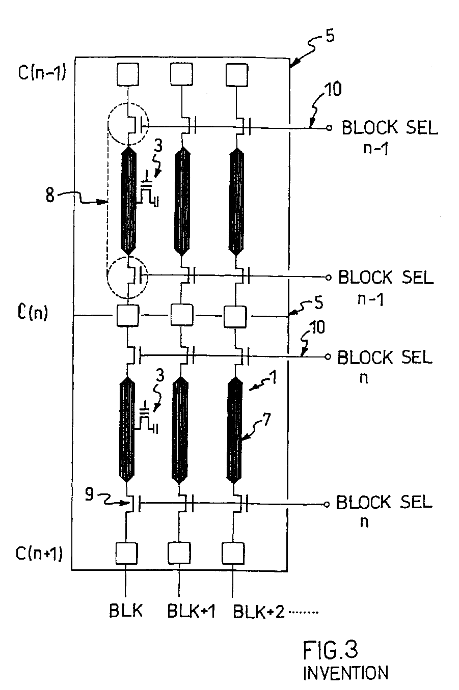
(57) An electronic memory device organized into sections which are in turn divided into
blocks (1) formed of cells (3) and their associated decoding and addressing circuits
(2), the cells being connected in a predetermined circuit configuration and each block
being included between two opposite contact regions (4) which are interconnected by
parallel continuous conduction lines referred to as the bit lines (7) . In the present
invention, at least one interruption is provided in each bit line (7) near a contact
region (4) by inserting a controlled switch (9) which functions as a block selector
(8).
Advantageously, the proposed solution allows each block to be isolated individually
by enabling or disabling as appropriate the switches (9) of the cascade connected
blocks (1).
Also provided is a method of implementing the memory block (1), as organized into
a matrix-like configuration, individually selectable from a plurality of blocks embedded
in a memory device, wherein each memory cell (3) is identified by a continuous bit
line (7) enabled by at least one block selector (8), by a broken bit line or 'segment'
(13) connected to the continuous one (7) through an address device (2), and by a word
line orthogonal to the direction of the bit lines, and formed on a substrate having
a first type fo conductivity.
|
|
