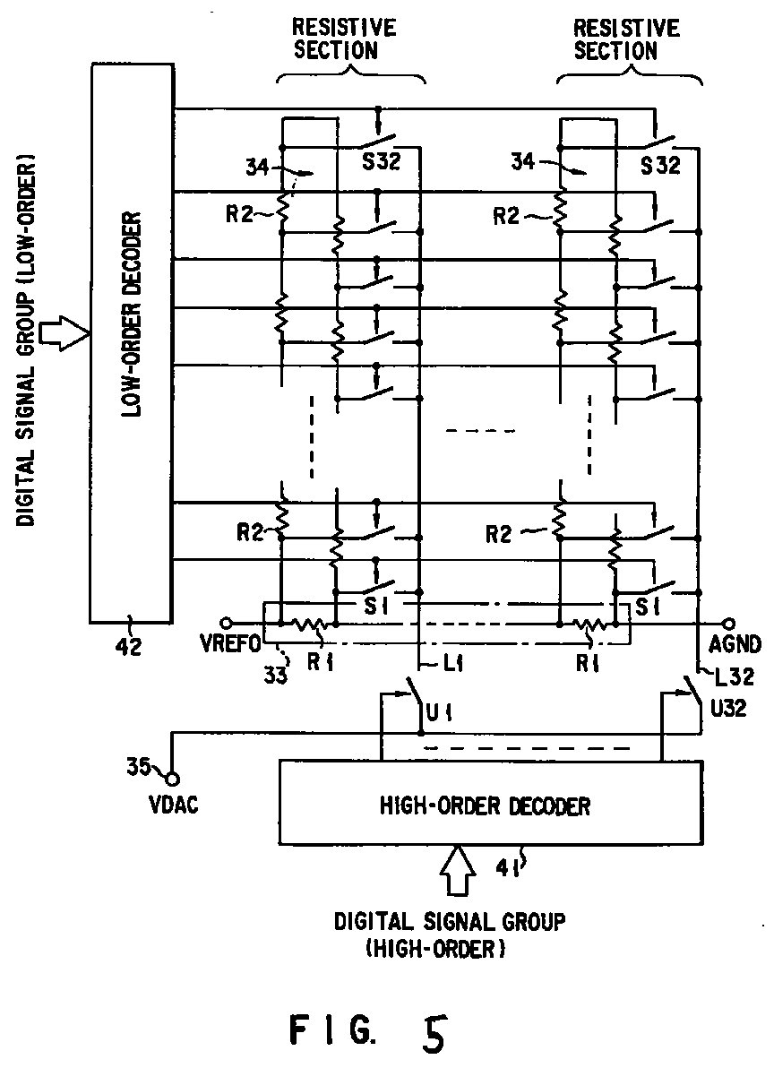
(57) A digital-to-analog conversion circuit includes a first reference voltage generation
circuit (33) for generating a plurality of first reference voltages, a plurality of
second reference voltage generation circuits (34) for generating a plurality of second
reference voltages created by dividing a difference in potential between adjacent
two of the first reference voltages, a first selective control circuit (31, SH1 to
SH32, SU) for, upon receiving a first digital input signal group, selecting one of
the first reference voltages and applying the selected one to a specified one (L1)
of a plurality of signal lines during a first period, and selecting all of second
reference voltages generated in one of the plurality of second reference voltage generation
circuits and applying all the selected second reference voltages to signal lines (L2
to L32) other than the specified signal line, respectively, during a second period
succeeding the first period, and a second selective control circuit (32, SD1 to SD32)
for, upon receiving a second digital input signal group, applying a voltage of the
specified signal line to an analog output terminal (35) during the first period, and
applying voltages of the signal lines other than the specified signal line to the
analog output terminal during the second period.
|
|
