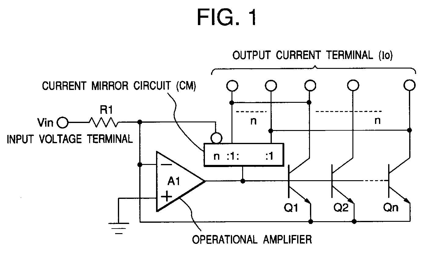
(57) This invention provides an absolute value voltage to current conversion circuit which
realizes multiple outputs of the current obtained by the conversion of a voltage.
For an input voltage of positive polarity, an inverting voltage to current conversion
circuit is formed by means of an operational amplifier and a multiple output current
mirror circuit. In that case, currents which are 1/n of a converted current are obtained
by setting the ratio of the input current to the output current of the current mirror
circuit to n:1. For an input voltage of negative polarity, a noninverting voltage
to current conversion circuit is formed by means of the operational amplifier and
a plurality, n, of bipolar transistors. The converted current is distributed among
n bipolar transistors to obtain an output current per transistor which is 1/n of the
converted current. As a result, an absolute value voltage to current conversion circuit
with multiple outputs can be realized.
|
|
