| (19) |
 |
|
(11) |
EP 0 864 229 B1 |
| (12) |
EUROPEAN PATENT SPECIFICATION |
| (45) |
Mention of the grant of the patent: |
|
26.01.2000 Bulletin 2000/04 |
| (22) |
Date of filing: 29.11.1996 |
|
| (51) |
International Patent Classification (IPC)7: H04N 9/04 |
| (86) |
International application number: |
|
PCT/GB9602/936 |
| (87) |
International publication number: |
|
WO 9720/434 (05.06.1997 Gazette 1997/24) |
|
| (54) |
OPTOELECTRONIC SENSOR WITH SHUFFLED READOUT
OPTOELEKTRONISCHER SENSOR MIT UNSORTIERUNG BEIM AUSLESEN
CAPTEUR OPTOELECTRONIQUE AVEC LECTURE REDISTRIBUEE
|
| (84) |
Designated Contracting States: |
|
DE FR GB IT NL |
| (30) |
Priority: |
29.11.1995 GB 9524337
|
| (43) |
Date of publication of application: |
|
16.09.1998 Bulletin 1998/38 |
| (73) |
Proprietor: VLSI VISION LIMITED |
|
Edinburgh EH12 8BD (GB) |
|
| (72) |
Inventors: |
|
- DENYER, Peter, Brian
Edinburgh EH10 5EA (GB)
- HURWITZ, Jonathan, Ephriam, David
Edinburgh EH9 1LS (GB)
- SMITH, Stewart, Gresty
Edinburgh EH10 4SA (GB)
|
| (74) |
Representative: Kerr, Sheila Agnes Fife et al |
|
Cruikshank & Fairweather,
19 Royal Exchange Square
Glasgow G1 3AE
Glasgow G1 3AE (GB) |
| (56) |
References cited: :
EP-A- 0 605 898
GB-A- 2 175 173
US-A- 5 194 944
|
DE-A- 3 828 867
US-A- 4 802 001
|
|
| |
|
|
|
|
| |
|
| Note: Within nine months from the publication of the mention of the grant of the European
patent, any person may give notice to the European Patent Office of opposition to
the European patent
granted. Notice of opposition shall be filed in a written reasoned statement. It shall
not be deemed to
have been filed until the opposition fee has been paid. (Art. 99(1) European Patent
Convention).
|
[0001] The present invention relates to integrated circuits (I.C.s) suitable for use as
image array sensors, and in particular, for use as multi-spectral image array sensors.
Such a multispectral image array sensor is described for example in US-A-5 194 944.
[0002] I.C. image array sensors are commonly used in solid state cameras and colour image
sensors are known which comprise a two-dimensional array of sensing cells which is
provided with a matrixed pattern of colour filters, for example, red, green and blue
filters. The array has a plurality of rows and columns of sensing cells and outputs
from the sensing cells are read out individually, row by row, at a single array output
the output of neighbouring cells being read sequentially. Horizontal and vertical
shift registers are normally used for this purpose. Cell outputs corresponding to
different colours are demultiplexed at the array output and fed to respective colour
channels.
[0003] Commonly, neighbouring sensing cells in the array have different colour filters in
order to achieve appropriate spatial sampling of radiation of each colour being sensed
for each colour channel of the sensor. Since the outputs of neighbouring cells are
read out sequentially, the cell outputs form a signal stream at the array output of
inherently fluctuating form due to the different colour radiation sensed by neighbouring
cells - even in image areas which have a constant colour across a number of neighbouring
cells, where that colour corresponds to different signal levels on the different colour
channels. This fluctuating signal results in one or more relatively high frequency
signal components at the array output whose amplitude is related to background chromaticity
as well as to image scene luminance.
[0004] Such high frequency signal component(s) lead to interference between neighbouring
sensing cell output signals and consequently to corruption of the image chromaticity
interpreted by circuits which follow the sensor, producing visual image error effects
in a camera in which the sensor is used. Moreover, if the sensing cell matrixed colour
filter pattern is not the same in all respects for each row of the array, then the
resulting chromaticity errors also differ from row to row, producing more visually
offensive image errors.
[0005] Additionally, the fluctuating signal stream at the array output including the associated
spurious high frequency signal components, can be difficult to handle in the analogue
domain in which such image array sensors normally operate.
[0006] It is an aim of the present invention to overcome or reduce one or more of the foregoing
disadvantages.
[0007] This object is achieved by the invention as set out in the claims.
[0008] One advantage of the integrated circuit according to claim 1 is that the sensing
cell outputs for the cells of at least two series, preferably each series, of cells
in said at least one row, can be read out consecutively at the array output. Thus,
the cell outputs from sensing cells for the same channel of said plurality of channels
can be read out consecutively. This minimises fluctuation in the array output signal
stream due to variations in individual cell output signals from cells formed and arranged
for sensing radiation of different wavelengths since the difference in radiation and
hence signal level between successive cells for the same channel are often much smaller
than the difference in radiation and hence signal level between neighbouring cells
for different channels.
[0009] The array of sensing cells may be a one-dimensional array having a single row of
sensing cells. Such an array may, for example, be suitable for use in an image scanning
device.
[0010] Preferably, the array is a two-dimensional array having a plurality of rows and columns
of sensing cells with a vertical scanning means also coupled to each cell in the array.
[0011] Adjacent sensing cells in each row may be formed and arranged for sensing radiation
of wavelengths corresponding to different ones of said plurality of channels. The
integrated circuit may be suitable for use as a colour image sensor wherein said plurality
of channels are for radiation corresponding to respective different colours. For example,
there may be three colour channels corresponding respectively to red, green and blue
radiation wavelengths. Each row may, for example, contain three series of sensing
cells, for sensing red, green and blue wavelength radiation respectively. The three
series of cells may be interspersed such that each row contains an alternating pattern
of red (R), green (G), and blue (b), sensing cells e.g. R G B R G B R G ... Alternatively,
each row may, for example, contain only two series of sensing cells. The two series
of cells in each row may be arranged so that every third cell senses a different colour
radiation to every first and second cell e.g. B B R B B R B B R... Said interspersed
series of sensing cells contained in any one row may comprise sensing cells for sensing
at least one different colour radiation to the sensing cells of the interspersed series
of cells in another row. For example, a first row may contain two series of cells
for sensing red and blue radiation and a second row may contain two series of cells
for sensing red and green radiation. Where each row contains two interspersed series
of cells, the array of cells may be arranged in a Bayer matrix pattern in which the
two series of cells in each odd-numbered row are interspersed to form an alternating
pattern of cells for sensing a first colour and a second colour, e.g. G R G R G R
..., and the two series of cells in each even-numbered row are interspersed to form
an alternating pattern of cells for sensing the first colour and a third colour, e.g.
B G B G B G ...
[0012] The integrated circuit may additionally be capable of sensing radiation at non-visible
wavelengths, for example, infra-red radiation. Thus, for example, at least one of
said plurality of channels may be for infra-red or other non-visible radiation and
some of the sensing cells may consequently be for sensing infra-red or other non-visible
radiation respectively.
[0013] The array of sensing cells may include a matrixed pattern of filters corresponding
to different radiation wavelengths so as to enable essentially similar sensing cells
to sense radiation at a particular wavelength, or over a particular band of wavelengths,
corresponding to a respective one of said plurality of channels. Alternatively there
could be cells having sensing surfaces responsive to different radiation wavelengths.
[0014] Preferred embodiments of the invention will now be described by way of example only
and with reference to the accompanying drawings in which:-
Fig. 1 depicts schematically the architecture of a known I.C. image array sensor;
Fig. 2 illustrates schematically a portion of a two-dimensional colour image sensor
array wherein the sensing cells are arranged according to a Bayer matrix;
Fig. 3 depicts the architecture of an I.C. image array sensor according to one aspect
of the present invention;
Fig. 4 illustrates schematically the layout and components of a solid state camera
system in which the sensor of Fig. 1 may be incorporated;
Fig. 5 depicts the architecture of an alternative I.C. image array sensor according
to the invention; and
Fig. 6 depicts a further alternative I.C. image array sensor architecture according
to another embodiment of the invention.
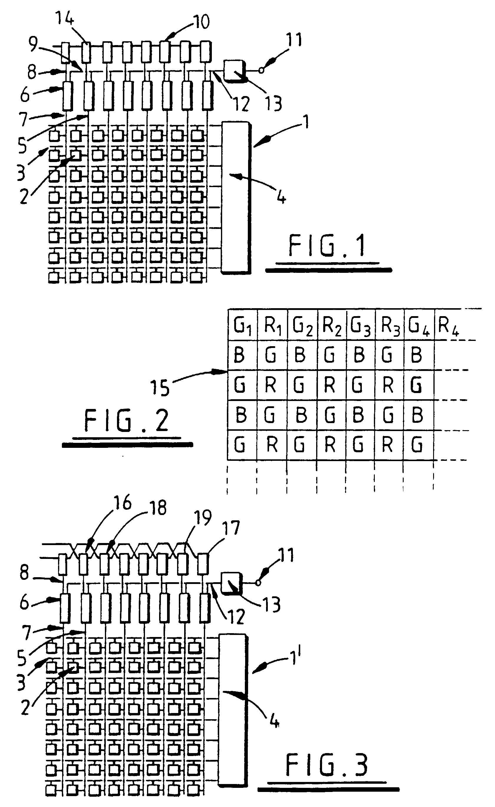
[0015] A known type of image array sensor 1 fabricated as an integrated circuit is illustrated
schematically in Fig. 1. Such a sensor is described in detail in our British Patent
No. 2 252 886 B. The sensor 1 consists of an array of pixels 2 laid out in generally
rectangular format in rows and columns. Each pixel 2 in a row is connected to a common
horizontal line called a word-line 3 and each word line is connected to digital circuitry
4 which is used to generate and drive the necessary pattern of row-select signals
along the word lines. This circuitry 4 generally takes the form of a vertical shift
register. Each vertical column of pixels is connected to a common conductor known
as a bitline 5 which is connected to a respective separate individual analogue switch
sense amplifier circuit 6 at the top of said column (as viewed in Fig. 1). The amplifier
circuit 6 has two inputs 7, 8 and one output 9. One input 8 is coupled to a horizontal
shift register 10 which produces enabling signals that control the analogue switch
sense amplifier circuits 6 to enable the signals on consecutive bit-lines to be connected
to a main output 11 of the array. The output 9 of each amplifier 6 is connected to
a common conductor 12 which functions as a common read out line and which is connected
to a sense amplifier 13. The amplifier 13 has an output which constitutes the main
array output 11.
[0016] The horizontal shift register 10 has a plurality of shift register elements 14 each
one of which is coupled to the input 8 of a respective one of the amplifier circuits
6. The sensor operates a "single channel" readout scheme in which pixel outputs are
read row by row and outputs from adjacent pixels in each row are read sequentially
by the horizontal shift register elements and fed to the main array output 11 to form
a signal stream of pixel outputs. To enable the integrated circuit to function as
a colour image array sensor the pixel array is treated with a matrixed pattern of
colour filters. Adjacent pixels have different colour filters so as to achieve satisfactory
spatial sampling of each colour type.
[0017] The signal stream at the main array output 11, consisting of sequential pixel outputs
for each row of the array, is demultiplexed, by additional circuitry (not shown) of
the integrated circuit, and interpolated to form synchronous parallel colour signals
for a plurality of corresponding colour channels of the sensor or, more specifically,
of the solid state camera system in which the sensor 1 is normally incorporated.
[0018] In one embodiment of this type of colour image array sensor the matrixed pattern
of colour filters is a Bayer matrix as described in US patent no. 3 971 065. A portion
15 of a Bayer matrix is shown schematically in Fig. 2, in which each row of the array
comprises two series of pixels, all the pixels of each series having the same colour
of filter, the colour filters of the pixels in each series being either red (R), green
(G) or blue (B), and the two series of pixels in each row being interspersed so as
to form an alternating two-colour pattern e.g. G R G R G R ... etc. The first and
every subsequent odd-numbered row have the pixel colour pattern G R G R G R... and
the second and every subsequent even-numbered row have the pixel colour pattern B
G B G B G ...
[0019] The Bayer matrix pixel array pattern shown in Fig. 2 has many favourable properties
for colour image reconstruction, but chromaticity errors are introduced to the reconstructed
image due to the single channel readout scheme in which all the pixels in each row
are output sequentially under the control of the horizontal shift register 10. For
example, row one of the array is output in the sequence G1, R1, G2, R2, G3, R3, G4,
R4... For an area of the image containing a cyan hue, for example, this sequence may
look like: 1, o, 1, 0, 1, 0, 1, 0... Such a sequence produces a spurious high frequency
signal at the Nyquist frequency (i.e. half the pixel sampling frequency), whose amplitude
is related to the background chromaticity, and which can also be difficult to handle
in the analogue domain.
[0020] Fig. 3 illustrates schematically an image array sensor 1' according to the present
invention in which the horizontal shift register 10 has been replaced by two horizontal
shift registers 16, 18. The other components of the sensor are the same or similar
to those shown in the sensor of Fig. 1 and are accordingly referenced using like numerals.
The array of pixels 2 follows the Bayer matrix pattern of filter colours shown in
Fig. 2. The plurality of shift register elements 17, 19 of the two horizontal shift
registers 16, 18 are interleaved alternately, and the shift register elements 17 of
one of the horizontal shift registers 16 are coupled to one series of like coloured
pixels in each row via respective alternate ones of the amplifier circuits 6 and the
shift register elements 19 of the other of the horizontal shift registers 18 are coupled
to the other one of the series of like-coloured pixels in each row via separate respective
ones of the amplifier circuits 6.
[0021] By first using one horizontal shift register 16 to read the alternate pixel outputs
corresponding to one colour of pixels in the first row, and then using the second
shift register 18 to read the pixel outputs of the other colour of pixels in that
row, the output signal stream for that row, at the main array output 11, becomes:
G1, G2, G3, G4 ..., R1, R2, R3, R4, ... For example, for a cyan hue this reads as:
1, 1, 1, 1, ..., 0, 0, 0, 0, ... The latter re-arranged or "shuffled" sequence eliminates
the spurious high frequency components associated with the known single horizontal
shift register arrangement of Fig. 1 and is generally easier to handle in the analogue
domain. Each row of pixel outputs is read in this manner, by the two horizontal shift
registers 16, 18 to produce a shuffled pixel output signal stream.
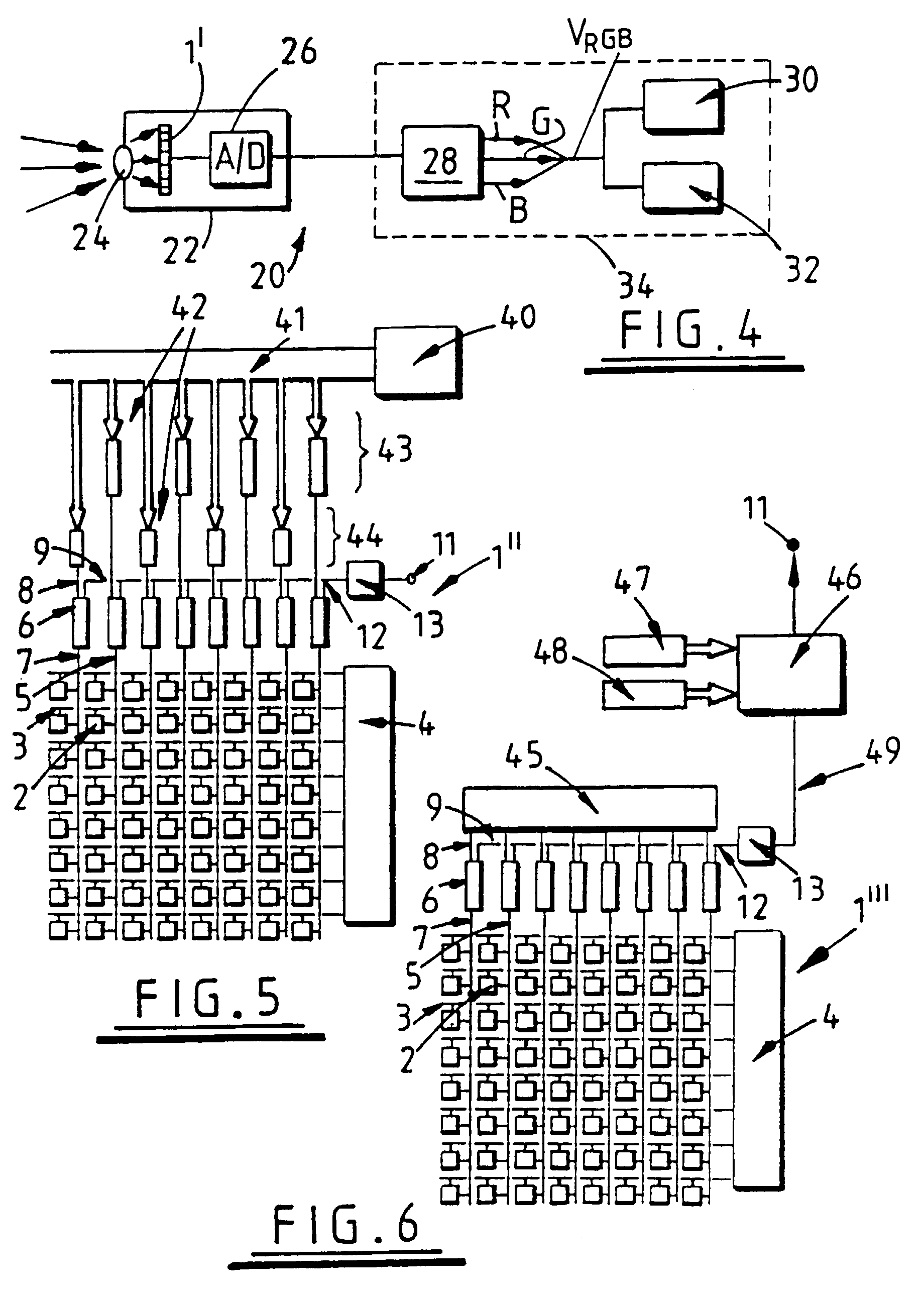
[0022] Fig. 4 shows schematically the layout of a solid state camera system 20 incorporating
the image array sensor of Fig. 3(referenced 1' in Fig. 4). The camera system includes
a camera head 22 comprising a lens 24 and the image array sensor 1'. The array is
read row-by-row, the shuffled signal stream of pixel outputs read out at the main
array output 11 of the sensor 1' being fed to an analogue to digital convertor 26
where the pixel outputs are converted from analogue to digital signals which are subsequently
fed to a signal processing unit 28 which is configured and/or programmed to demultiplex
the shuffled pixel output streams into red green and blue colour channels (R.G.B)
of a video signal V
RGB which is output by the processing unit 28 to a video display unit 30, and/or a recording
device 32, coupled to the processing unit 28. (The processing unit preferably also
interpolates the red, green and blue channel signals to form synchronous, parallel
colour channel signals for the video signal V
RGB before being output to the display unit 30, and/or recording device 32.) In the embodiment
illustrated in Fig. 4 the processing unit 28 is provided on a second integrated circuit
which is provided together with the display unit 30 and/or recording device 32 in
an image processing unit or module 34 (indicated in broken lines in Fig. 4) of the
camera system 20 for use with the camera head 22. The A/D convertor 26 is provided
in circuitry incorporated in the camera head 22, (which could, if desired, be integrally
provided in the image sensor integrated circuit 1'). The second integrated circuit
may also include colour balance control circuitry and/or exposure control circuitry
of the camera system.
[0023] It is envisaged that the camera head 22 need not always be used with the image processing
unit 34 shown in the camera system of Fig. 4. It would be possible, for example, for
image data output from the image sensor 1' in the camera head 22 to be fed straight
to a recording device where the shuffled output signal streams would be recorded on
a recording medium (e.g. a computer hard disk, or a floppy disk). The recorded image
data (in its shuffled output signal stream form) would be demultiplexed into colour
channels to form a video signal and/or image at a later date by reading the recorded
data into a suitably programmed processor.
[0024] In an alternative embodiment (not shown) the A/D convertor 26 is incorporated in
the image processing unit 34, rather than in the camera head. Similarly, in a further
possible embodiment (not shown) A/D conversion and some, or all, of the signal processing
performed by the processing unit 28 is carried out in the camera head 22. This may
be done, for example, by processing circuitry included on the same chip as that on
which the integrated circuit image array sensor 1' is formed. The processing circuitry
on the chip may thus be configured to digitally format the image data output from
the sensor 1' and to convert the formatted data into a standard video form which can
be input directly to a video display unit and/or recorder device, or stored in an
external memory for future use. Alternatively, the processing circuitry on the chip
may be configured to convert the image data output from the sensor 1' into a particular
digital format, the formatted data then being output from the camera head 22 to further
external signal processing circuitry which is programmed, or configured, to interpret
the formatted data and produce therefrom a standard video signal (e.g. in three channel
R, G, B form) for use as before.
[0025] It will be appreciated that the number of horizontal shift registers may be chosen
according to the type of colour pixel array pattern which is used in the sensor. For
example, where three colours of pixel are disposed in each row to form three interspersed
series of pixels, the horizontal shift registers may be used so as to read the pixel
outputs for each series of like-coloured pixels consecutively e.g. G, G, G, ..., R,
R, R, ..., B, B, B, ...
[0026] It will also be appreciated that the invention is suitable for multi-spectral sensors
in which some of the pixels are treated so as to sense non-visible radiation which
may, for example, be infra-red radiation.
[0027] The invention is also applicable to one-dimensional image array sensors in which
there is a single row of different colour pixels. (In such an embodiment, no vertical
shift register 4 is necessary).
[0028] It will moreover be appreciated that further modifications and variations are possible
without departing from the scope of the invention. For example, the pixel array may
incorporate only pixels treated with cyan, magenta and yellow filters. Each row may
also contain one or more additional pixels for use in measuring light intensity or
another reference quantity which may be of interest, although the number of such pixels
in each row will normally be relatively small.
[0029] Fig. 5 illustrates an alternative embodiment of the invention in which an address
decode system is used instead of the interleaved shift registers 16,18 of the Fig.
3 embodiment. Like components of the sensors shown in Figs. 3 and 5 are referenced
by like numerals. In the sensor 1" of Fig. 5, an address generator 40 generates a
sequence of addresses 41 which are decodable by decode elements 42 coupled to the
top of the pixel columns 5. The address generator 40 and decode elements 42 are arranged
to read out the pixel output signals, row-by-row, reading out groups of like-coloured
pixels consecutively to achieve the same effect as in Fig. 3, where the two horizontal
shift registers were used. In a Bayer matrix array therefore, the shuffled output
signal stream for each row is made up of the outputs from two colours of pixel e.g.
R, G shuffled into like-coloured groupings R, R, R, ......., G, G, G, ....... As indicated
in Fig. 5, a decode element 42 is coupled to the top of each column, there thus being
two sets of decode elements: one set 43 linked to alternate pixels in each row having
one colour, and the other set 44 linked to alternate pixels in each row having another
colour.
[0030] Fig. 6 shows another possible embodiment of the invention in which a sensor 1" uses
another "shuffling" technique to obtain the desired shuffled output signal streams
from each row of the array. In this embodiment, each row of pixels 2 in the array
is read out sequentially by read out means 45 which may comprise one or more shift
registers, or alternatively, address decode circuitry, for reading the pixels sequentially.
The pixel output signal stream from each row output from the common read out line
12 and the sense amplifier 13 is input to a memory circuit 46 which is included in
the output path 49 of the sensor 1", between the amplifier 13 and the main array output
11. This memory circuit 46 is accessed by an input addressing means 48, and an output
addressing means 47, so as to order the pixel output signals for each row into like-coloured
pixel groups, thereby obtaining similar shuffled output signal streams as with the
Figs. 3 and 5 embodiments. The memory circuit 46 may consist of purely analogue storage
means, or may be achieved through Analog-Digital conversion followed by digital storage
means.
1. An integrated circuit CMOS multi-spectral image array sensor for use in a solid state
camera system having a plurality of channels for radiation of different wavelengths,
the sensor comprising an array of sensing cells having at least one row of sensing
cells, each sensing cell being formed and arranged for sensing radiation corresponding
to one of said channels, said at least one row containing a plurality of series of
sensing cells which series are interspersed with each other in a predetermined manner,
each series consisting essentially of sensing cells for a respective one of said plurality
of channels, and read out means for reading signal outputs from the cells in said
at least one cell row of the array, wherein said read out means is adapted to read
out consecutively, in use of the sensor, the signal outputs from the sensing cells
in each one of said plurality of series of cells in said at least one row, via a single
common read out line coupled to the sensing cells in each one of said plurality of
series of cells.
2. An integrated circuit CMOS sensor according to claim 1, wherein said read out means
comprises an address decode system which is configured to read consecutively the outputs
from the sensing cells in each one of said plurality of series of cells in said at
least one row of the array.
3. An integrated circuit CMOS sensor according to claim 1, wherein said read out means
comprises horizontal scanning means coupled to each cell in the array for scanning
said at least one cell row of the array, and wherein said horizontal scanning means
comprises at least two horizontal shift register means, each said horizontal shift
register means being coupled to the cells of a respective one of said plurality of
interspersed series of cells.
4. An integrated circuit CMOS sensor according to claim 1, wherein the sensing cells
in each one of said plurality of series of cells in said at least one row are coupled
indirectly to said single common read out line via amplifier means.
5. An integrated circuit CMOS sensor according to any of claims 1 to 4, wherein the array
of sensing cells is a one-dimensional array having a single row of sensing cells.
6. An integrated circuit CMOS sensor according to any of claims 1 to 4, wherein the array
is a two-dimensional array having a plurality of rows and columns of sensing cells
and the sensor further includes vertical scanning means.
7. An integrated circuit CMOS sensor according to claim 6 wherein each row of cells of
said two-dimensional array contains a plurality of series of sensing cells which series
are interspersed with each other in a predetermined manner, each series consisting
essentially of sensing cells for a respective one of said plurality of channels.
8. An integrated circuit CMOS sensor according to claim 7 wherein each row contains the
same number of interspersed series of sensing cells.
9. An integrated circuit CMOS sensor according to claim 6 or claim 7 wherein said plurality
of series of cells contained in each row are interspersed in the same predetermined
manner.
10. An integrated circuit CMOS sensor according to any of claims 5 to 9, as dependent
from claim 3, wherein the number of horizontal shift register means provided is equal
to the number of said interspersed series of cells in said at least one row.
11. An integrated circuit CMOS sensor according to any of claims 5 to 10, as dependent
from claim 3, wherein each said horizontal shift register means comprises at least
one horizontal shift register.
12. An integrated circuit CMOS sensor according to claim 11, wherein each said horizontal
shift register comprises a plurality of shift register elements each of which elements
is coupled, via a respective switch sense amplifier means, to a respective one of
the sensing cells in said at least one row of the array, each said switch sense amplifier
means being coupled to said single common read out line.
13. An integrated circuit CMOS sensor according to claim 12, wherein the shift register
elements of said horizontal shift registers of said at least two horizontal shift
register means are interleaved whereby a compact arrangement of said horizontal shift
registers in the sensor is achieved.
14. An integrated circuit CMOS sensor according to claim 6 wherein each said row of sensing
cells contains two interspersed series of cells, the two series of cells in each row
being interspersed to form an alternating pattern.
15. An integrated circuit CMOS sensor according to any preceding claim wherein each said
series of sensing cells consists essentially of cells for sensing visible radiation
of one particular colour.
16. An integrated circuit CMOS sensor according to claim 15 when dependent from claim
14, wherein the two series of cells in each odd-numbered row are interspersed to form
an alternating pattern of cells for sensing a first colour and a second colour and
the two series of cells in each even-numbered row are interspersed to form an alternating
pattern of cells for sensing said first colour and a third colour.
17. An integrated circuit CMOS sensor according to claim 14 or claim 16 wherein there
are provided two said horizontal shift register means for reading the outputs from
the sensing cells of respective ones of said two interspersed series of cells in every
row of the array.
18. An integrated circuit CMOS sensor according to any preceding claim wherein the sensor
is capable of sensing infra-red radiation.
19. An integrated circuit CMOS sensor according to any preceding claim wherein said sensing
cells comprise pixels having sensing surfaces responsive to different predetermined
radiation wavelengths.
20. An integrated circuit CMOS sensor according to any of claims 1 to 15 wherein said
sensing cells comprise pixels provided with respective filters for enabling said pixels
to sense radiation corresponding to different wavelengths.
21. An integrated circuit CMOS sensor according to any preceding claim wherein each said
sensing cell is capable of sensing radiation over a predetermined band of wavelengths.
22. An integrated circuit CMOS sensor according to claim 20 or 21 wherein said array of
sensing cells comprises an array of pixels provided with a matrixed pattern of red,
green and blue colour filters.
23. An integrated circuit CMOS sensor according to claim 21 or claim 22 wherein said array
of sensing cells comprises an array of pixels provided with a matrixed pattern of
cyan, magenta and yellow colour filters.
24. An integrated circuit CMOS sensor according to any preceding claim wherein said array
of sensing cells contains at least one sensing cell for use in sensing light intensity.
25. A method of reading outputs of individual sensing cells of an array of sensing cells
fabricated in an integrated circuit CMOS multi-spectral image array sensor for use
in a solid state camera system having a plurality of channels for radiation of different
wavelengths, the array comprising at least one row of sensing cells, said at least
one row containing a plurality of series of sensing cells which series are interspersed
with each other in a predetermined manner and each series consisting essentially of
sensing cells for a respective one of said plurality of channels, and read out means
for reading signal outputs from the cells in said at least one cell row of the array,
wherein the method comprises reading out consecutively sensing cell output signals
from the sensing cells in each one of said plurality of series of cells in said at
least one row, via a single common read out line coupled to the sensing cells in each
one of said plurality of series of cells.
26. A method according to claim 25, wherein separate horizontal shift register means are
used to read the cell output signals from the cells of respective ones of said plurality
of interspersed series of cells in said at least one row.
27. A method according to claim 25 or claim 26, wherein the array of sensing cells is
a two-dimensional array having a plurality of rows and columns, each row containing
a plurality of series of sensing cells which series are interspersed with each other
in a predetermined manner, each series consisting essentially of sensing cells for
a respective one of said plurality of channels, and the method comprises reading consecutively
the sensing cell output signals from the cells in each one of said plurality of series
of cells in each row.
28. A method according to any of claims 25 to 27, wherein said single common read out
line is connected to a respective single output of the array and wherein sensing cell
output signals from the cells in each one of said plurality of series of cells in
said at least one row are read consecutively into signal processing means coupled
to said output of the array and which are adapted to demultiplex said sensing cell
output signals into respective ones of said plurality of channels for radiation of
different wavelengths.
29. A method according to claim 28, wherein said sensing cell output signals are analogue
signals which are converted to digital signals before being demultiplexed into said
plurality of channels.
30. A method according to any of claims 25 to 29, wherein said single common read out
line is connected to a respective single output of the array and wherein sensing cell
output signals from the cells in each one of said plurality of series of cells in
said at least one row are read consecutively into a data recording means connected
to said output of the array, for recording said consecutively arranged sensing cell
output signals from the cells in each one of said plurality of series of cells.
31. A solid state camera head incorporating at least one lens and an integrated circuit
sensor according to any of claims 1 to 24.
32. A solid state camera system having a plurality of channels for radiation of different
wavelengths, incorporating an integrated circuit CMOS sensor according to any of claims
1 to 24.
33. A solid state camera system according to claim 32, further including signal processing
means adapted to receive the sensing cell output signals read consecutively from the
cells in each one of said plurality of series of cells in the or each said row and
demultiplex them into respective ones of said plurality of channels for radiation
of different wavelengths.
34. A solid state camera system according to claim 33, wherein said sensing cell output
signals are analogue signals and the system further includes analogue to digital (A/D)
signal converter means for converting said analogue signals to digital signal which
are received by said signal processing means.
35. A solid state camera system according to claim 34 wherein said A/D signal converter
means are included in said integrated circuit CMOS sensor.
36. Signal processing means suitable for use in a solid state CMOS camera system and adapted
to receive and demultiplex streams of output signals from sensing cells of an integrated
circuit CMOS multi-spectral image sensing array of the camera system, said array having
at least one row of sensing cells containing a plurality of series of sensing cells
interspersed in a predetermined manner, each series consisting essentially of sensing
cells for a respective one of a plurality of channels for radiation of different wavelengths
in the solid state camera system, said signal processing means being adapted to demultiplex
a shuffled stream of output signals from sensing cells in said at least one row into
respective ones of said plurality of channels, in which shuffled stream of output
signals the output signals from the sensing cells in each one of said plurality of
series of cells in said at least one row are arranged consecutively, and are read
out via a single common read out line coupled to the sensing cells.
37. Signal processing means according to claim 36, adapted to receive streams of output
signals from each row of a two-dimensional image sensing array of the solid state
camera system, each row comprising a plurality of series of sensing cells interspersed
with each other in a predetermined manner and each series consisting essentially of
sensing cells for a respective one of said plurality of channels, said signal processing
means being adapted to demultiplex a shuffled stream of sensing cell output signal
from each row into respective ones of said plurality of channels, wherein in each
shuffled stream of output signals the output signals from the sensing cells in each
one of said plurality of series of cells in the respective row are arranged consecutively.
1. Multispektraler Bild Matrixfeldsensor in integrierter CMOS-Halbleiterschaltung zur
Verwendung in einem Halbleiter-Kamerasystem mit einer Mehrzahl von Kanälen für Strahlung
verschiedener Wellenlängen, wobei der Sensor ein Matrixfeld von Sensorzellen enthält,
das wenigstens eine Zeile von Sensorzellen hat, wobei jede Sensorzelle zum Lesen von
Strahlung entsprechend einem der Kanäle gebildet und angeordnet ist, wobei die wenigstens
eine Zeile eine Mehrzahl von Sensorzellenreihen enthält, wobei die Reihen untereinander
in einer vorbestimmten Weise verteilt sind, wobei jede Reihe im wesentlichen aus Sensorzellen
für einen jeweiligen der Mehrzahl von Kanälen besteht, und wobei der Sensor eine Ausleseeinrichtung
zum Lesen von Signalausgängen von den Zellen in der wenigstens einen Zellenreihe des
Matrixfeldes enthält, wobei die Ausleseeinrichtung dazu eingerichtet ist, bei Verwendung
des Sensors die Signalausgänge von den Sensorzellen in jeder der Mehrzahl von Zellenreihen
in der wenigstens einen Zeile über eine einzige, gemeinsame Ausleseleitung aufeinander
folgend auszulesen, die mit den Sensorzellen in jeder der Mehrzahl von Zellenreihen
verbunden ist.
2. Integrierter CMOS-Sensor gemäß Anspruch 1, wobei die Ausleseeinrichtung ein Adress-Dekodiersystem
enthält, das konfiguriert ist, um die Ausgänge von den Sensorzellen in jeder der Mehrzahl
von Zellenreihen in der wenigstens einen Zeile des Matrixfeldes aufeinander folgend
auszulesen.
3. Integrierter CMOS-Sensor gemäß Anspruch 1, wobei die Ausleseeinrichtung eine horizontale
Scan-Einrichtung enthält, die an jede Zelle in dem Matrixfeld zum Scannen der wenigstens
einen Zellenzeile des Matrixfeldes gekoppelt ist, und wobei die horizontale Scan-Einrichtung
wenigstens zwei horizontale Schieberegistereinrichtungen enthält, wobei jede der horizontalen
Schieberegistereinrichtungen mit den Zellen einer jeweiligen der Mehrzahl von untereinander
verteilten Zellenreihen verbunden ist.
4. Integrierter CMOS-Sensor gemäß Anspruch 1, wobei die Sensorzellen in jeder der Mehrzahl
von Zellenreihen in der wenigstens einen Zeile indirekt an die einzige, gemeinsame
Ausleseleitung über eine Verstärkereinrichtung gekoppelt ist.
5. Integrierter CMOS-Sensor gemäß irgendeinem der Ansprüche 1-4, wobei das Matrixfeld
der Sensorzellen ein eindimensionales Matrixfeld mit einer einzigen Zeile von Sensorzellen
ist.
6. Integrierter CMOS-Sensor gemäß irgendeinem der Ansprüche 1-4, wobei das Matrixfeld
ein zweidimensionales Matrixfeld mit einer Mehrzahl von Zeilen und Spalten von Sensorzellen
ist, und der Sensor darüber hinaus eine vertikale Scan-Einrichtung enthält.
7. Integrierter CMOS-Sensor gemäß Anspruch 6, wobei jede Zellenzeile des zweidimensionalen
Matrixfeldes eine Mehrzahl von Sensorzellenreihen enthält, wobei die Reihen untereinander
auf eine vorbestimmte Weise verteilt sind, und wobei jede Reihe im wesentlichen aus
Sensorzellen für einen jeweiligen der Mehrzahl von Kanälen besteht.
8. Integrierter CMOS-Sensor gemäß Anspruch 7, wobei jede Zeile dieselbe Anzahl von untereinander
verteilten Reihen von Sensorzellen enthält.
9. Integrierter CMOS-Sensor gemäß Anspruch 6 oder Anspruch 7, wobei die Mehrzahl von
in jeder Zeile enthaltenen Zellenreihen auf dieselbe, vorbestimmte Weise untereinander
verteilt sind.
10. Integrierter CMOS-Sensor gemäß irgendeinem der Ansprüche 5-9, soweit von Anspruch
3 abhängig, wobei die Anzahl von vorgesehenen horizontalen Schieberegistereinrichtungen
gleich ist mit der Anzahl der untereinander verteilten Zellenreihen in der wenigstens
einen Zeile.
11. Integrierter CMOS-Sensor gemäß irgendeinem der Ansprüche 5-10, soweit von Anspruch
3 abhängig, wobei jede horizontale Schieberegistereinrichtung wenigstens ein horizontales
Schieberegister enthält.
12. Integrierter CMOS-Sensor gemäß Anspruch 11, wobei jedes horizontale Schieberegister
eine Mehrzahl von Schieberegisterelementen enthält, wobei jedes Element über eine
entsprechende Umschalt-Leseverstärkereinrichtung an eine entsprechende der Sensorzellen
in der wenigstens einen Zeile des Matrixfeldes gekoppelt ist, wobei jede Umschalt-Leseverstärkereinrichtung
an die einzige, gemeinsame Ausleseleitung gekoppelt ist.
13. Integrierter CMOS-Sensor gemäß Anspruch 12, wobei die Schieberegisterelemente der
horizontalen Schieberegister der wenigstens zwei horizontalen Schieberegistereinrichtungen
verschachtelt sind, wodurch eine kompakte Anordnung der horizontalen Schieberegister
in dem Sensor erreicht wird.
14. Integrierter CMOS-Sensor gemäß Anspruch 6, wobei jede Zeile der Sensorzellen zwei
untereinander verteilte Zellenreihen enthält, wobei die zwei Zellenreihen in jeder
Zeile untereinander verteilt sind, um ein abwechselndes Muster zu bilden.
15. Integrierter CMOS-Sensor gemäß irgendeinem der vorstehenden Ansprüche, wobei jede
Reihe von Sensorzellen im wesentlichen aus Zellen zum Lesen von sichtbarer Strahlung
einer bestimmten Farbe besteht.
16. Integrierter CMOS-Sensor gemäß Anspruch 15, soweit von Anspruch 14 abhängig, bei dem
die beiden Zellenreihen in jeder ungeradzahligen Zeile untereinander verteilt sind,
um ein abwechselndes Muster von Zellen zum Lesen einer ersten Farbe und einer zweiten
Farbe zu bilden, und die beiden Zellenreihen in jeder geradzahligen Zeile untereinander
verteilt sind, um ein abwechselndes Muster von Zellen zum Lesen der ersten Farbe und
einer dritten Farbe zu bilden.
17. Integrierter CMOS-Sensor gemäß Anspruch 14 oder Anspruch 16, bei dem zwei horizontale
Schieberegistereinrichtungen zum Lesen der Ausgänge von den Sensorzellen von jeweiligen
der untereinander verteilten Zellenreihen in jeder Zeile des Matrixfeldes vorgesehen
sind.
18. Integrierter CMOS-Sensor gemäß irgendeinem der vorstehenden Ansprüche, wobei der Sensor
fähig ist, Infrarotstrahlung zu lesen.
19. Integrierter CMOS-Sensor gemäß irgendeinem der vorstehenden Ansprüche, wobei die Sensorzellen
Pixel enthalten, die Sensorflächen aufweisen, die auf verschiedene, vorgegebene Strahlungswellenlängen
ansprechen.
20. Integrierter CMOS-Sensor gemäß irgendeinem der Ansprüche 1-15, wobei die Sensorzellen
Pixel enthalten, die mit entsprechenden Filtern versehen sind, um die Pixel zu befähigen,
Strahlung entsprechend verschiedener Wellenlängen zu lesen.
21. Integrierter CMOS-Sensor gemäß irgendeinem der vorstehenden Ansprüche, wobei jede
Sensorzelle fähig ist, Strahlung über ein vorbestimmtes Wellenlängenband hinweg zu
fühlen.
22. Integrierter CMOS-Sensor gemäß Anspruch 20 oder 21, wobei das Matrixfeld von Sensorzellen
ein Matrixfeld von Pixeln enthält, das mit einem matrixartigen Muster von Rot-, Grün-
und Blau-Farbfiltern versehen ist.
23. Integrierter CMOS-Sensor gemäß Anspruch 21 oder Anspruch 22, wobei das Matrixfeld
der Sensorzellen ein Matrixfeld von Pixeln enthält, das mit einem matrixförmigen Muster
von Cyan-, Magenta- und Gelb-Farbfiltern versehen ist.
24. Integrierter CMOS-Sensor gemäß irgendeinem der vorstehenden Ansprüche, wobei das Matrixfeld
der Sensorzellen wenigstens eine Sensorzelle zur Verwendung beim Ablesen der Lichtintensität
enthält.
25. Verfahren zum Lesen von Ausgängen einzelner Sensorzellen eines Matrixfeldes von Sensorzellen,
hergestellt in einem multispektralen Bild-Matrixfeldsensor in integrierter CMOS-Halbleiterschaltung
zur Verwendung in einem Halbleiter-Kamerasystem mit einer Mehrzahl von Kanälen für
die Strahlung verschiedener Wellenlängen, wobei das Matrixfeld wenigstens eine Zeile
von Sensorzellen enthält, wobei wenigstens eine Zeile eine Mehrzahl von Reihen von
Sensorzellen enthält, wobei die Reihen untereinander in einer vorbestimmten Weise
verteilt sind, und jede Reihe im wesentlichen aus Sensorzellen für einen entsprechenden
der Mehrzahl von Kanälen besteht, und wobei das Matrixfeld eine Ausleseeinrichtung
zum Auslesen von Signalausgängen von den Zellen in der wenigstens einen Zellenzeile
des Matrixfeldes enthält, wobei das Verfahren enthält, die Sensorzellen-Ausgangssignale
von den Sensorzellen in jeder der Mehrzahl von Zellenreihen in wenigstens einer Zeile
über eine einzige, gemeinsame Ausleseleitung aufeinander folgend auszulesen, wobei
die gemeinsame Ausleseleitung an die Sensorzellen in jeder der Mehrzahl von Zellenreihen
gekoppelt ist.
26. Verfahren gemäß Anspruch 25, bei dem separate, horizontale Schieberegistereinrichtungen
zum Auslesen der Zellenausgangssignale von den Zellen von jeweiligen der Mehrzahl
von untereinander verteilten Zellenreihen in wenigstens einer Zeile verwendet werden.
27. Verfahren gemäß Anspruch 25 oder Anspruch 26, wobei das Matrixfeld von Sensorzellen
ein zweidimensionales Matrixfeld mit einer Mehrzahl von Zeilen und Spalten ist, wobei
jede Zeile eine Mehrzahl von Reihen von Sensorzellen enthält, wobei die Reihen untereinander
auf eine vorbestimmte Weise verteilt sind, wobei jede Reihe im wesentlichen aus Sensorzellen
für einen jeweiligen der Mehrzahl von Kanälen besteht, und das Verfahren enthält,
die Sensorzellen-Ausgangssignale von den Zellen in jeder der Mehrzahl von Reihen von
Zellen in jeder Zeile aufeinander folgend auszulesen.
28. Verfahren gemäß irgendeinem der Ansprüche 25 bis 27, wobei die einzige, gemeinsame
Ausleseleitung mit einem entsprechenden, einzigen Ausgang des Matrixfeldes verbunden
ist, und wobei die Sensorzellen-Ausgangssignale von den Zellen in jeder der Mehrzahl
von Zellenreihen in der wenigstens einen Zeile aufeinander folgend in eine Signalverarbeitungseinrichtung
hinein gelesen werden, die an den Ausgang des Matrixfeldes gekoppelt und dafür eingerichtet
ist, die Sensorzellen-Ausgangssignale in entsprechende der Mehrzahl von Kanälen für
die Strahlung verschiedener Wellenlängen zu demultiplexen.
29. Verfahren gemäß Anspruch 28, bei dem die Sensorzellen-Ausgangssignale analoge Signale
sind, die vor dem Demultiplexen in die Mehrzahl von Kanäle in digitale Signale umgesetzt
werden.
30. Verfahren gemäß irgendeinem der Ansprüche 25 bis 29, bei dem die einzige, gemeinsame
Ausleseleitung mit einem entsprechenden, einzigen Ausgang des Matrixfeldes verbunden
ist, und bei dem die Sensorzellen-Ausgangssignale von den Zellen in jeder der Mehrzahl
von Zellenreihen in der wenigstens einen Zeile aufeinander folgend in eine Datenaufzeichnungseinrichtung
eingelesen werden, die mit dem Ausgang des Matrixfeldes verbunden ist, zum Aufzeichnen
der aufeinander folgend angeordneten Sensorzellen-Ausgangssignale von den Zellen in
jeder der Mehrzahl von Zellenreihen.
31. Halbleiterkamerakopf, in den wenigstens eine Linse und ein integrierter Sensor gemäß
irgendeinem der Ansprüche 1 bis 24 eingebaut sind.
32. Ein Halbleiterkamerasystem mit einer Mehrzahl von Kanälen für die Strahlung verschiedener
Wellenlängen, in das ein integrierter CMOS-Sensor gemäß irgendeinem der Ansprüche
1 bis 24 eingebaut ist.
33. Halbleiterkamerasystem gemäß Anspruch 32, weiter enthaltend eine Signalverarbeitungseinrichtung,
die dazu eingerichtet ist, die aufeinander folgend von den Zellen in jeder der Mehrzahl
von Zellenreihen in der oder jeder Zeile gelesenen Sensorzellen-Ausgangssignale zu
empfangen und sie in entsprechende der Mehrzahl von Kanälen für die Strahlung verschiedener
Wellenlängen zu demultiplexen.
34. Halbleiterkamerasystem gemäß Anspruch 33, bei dem die Sensorzellen-Ausgangssignale
analoge Signale sind, und das System weiter eine Analog-Digital-Signalumsetzeinrichtung
zum Umsetzen der analogen Signale in digitale Signale enthält, die von der Signalverarbeitungseinrichtung
empfangen werden.
35. Halbleiterkamerasystem gemäß Anspruch 34, bei dem die A/D-Signalumsetzeinrichtung
in dem integrierten CMOS-Sensor enthalten ist.
36. Signalverarbeitungseinrichtung, geeignet zur Verwendung in einem Halbleiter-CMOS-Kamerasystem
und eingerichtet zum Empfangen und Demultiplexen von Strömen von Ausgangssignalen
von Sensorzellen eines integrierten CMOS multispektralen Bildsensor-Matrixfeldes des
Kamerasystems, wobei das Matrixfeld wenigstens eine Zeile von Sensorzellen aufweist,
die eine Mehrzahl von Reihen von Sensorzellen enthält, die auf eine vorbestimmte Weise
untereinander verteilt sind, wobei jede Reihe im wesentlichen aus Sensorzellen für
einen jeweiligen der Mehrzahl von Kanälen für die Strahlung verschiedener Wellenlängen
in dem Halbleiter-Kamerasystem besteht, wobei die Signalverarbeitungseinrichtung dazu
eingerichtet ist, einen umsortierten Strom von Ausgangssignalen von Sensorzellen in
der wenigstens einen Zeile in entsprechende der Mehrzahl von Kanälen zu demultiplexen,
wobei in dem umsortierten Strom von Ausgangssignalen die Ausgangssignale von den Sensorzellen
in jeder der Mehrzahl von Zellenreihen in der wenigstens einen Zeile aufeinander folgend
angeordnet sind, und über eine einzige, gemeinsame, an die Sensorzellen gekoppelte
Ausleseleitung ausgelesen werden.
37. Signalverarbeitungseinrichtung gemäß Anspruch 36, dazu eingerichtet, Ströme von Ausgangssignalen
von jeder Zeile eines zweidimensionalen Bildsensor-Matrixfeldes des Halbleiter-Kamerasystems
zu empfangen, wobei jede Zeile eine Mehrzahl von Reihen von Sensorzellen enthält,
die untereinander auf eine vorbestimmte Weise verteilt sind und wobei jede Reihe im
wesentlichen aus Sensorzellen für einen jeweiligen der Mehrzahl von Kanälen besteht,
wobei die Signalverarbeitungseinrichtung dazu eingerichtet ist, einen umsortierten
Strom von Sensorzellen-Ausgangssignalen von jeder Reihe in entsprechende der Mehrzahl
von Kanälen zu demultiplexen, wobei in jedem umsortierten Strom von Ausgangssignalen
die Ausgangssignale von den Sensorzellen in jeder der Mehrzahl von Zellenreihen in
der jeweiligen Reihe aufeinander folgend angeordnet sind.
1. Capteur à réseau d'image multispectral CMOS à circuit intégré pour une utilisation
dans un système de caméra à l'état solide comportant une pluralité de canaux pour
le rayonnement de différentes longueurs d'onde, le capteur comprenant un réseau de
cellules de détection comportant au moins une rangée de cellules de détection, chaque
cellule de détection étant formée et agencée pour détecter un rayonnement correspondant
à l'un desdits canaux, ladite au moins une rangée contenant une pluralité de séries
de cellules de détection, lesquelles séries sont réparties de façon imbriquée d'une
manière prédéterminée, chaque série étant constituée essentiellement par des cellules
de détection pour celui respectif de ladite pluralité de canaux, et des moyens de
lecture pour lire des sorties de signal en provenance des cellules dans ladite au
moins une rangée de cellules du réseau, dans lequel lesdits moyens de lecture sont
adaptés pour lire de façon consécutive, lors de l'utilisation du capteur, les sorties
de signal en provenance des cellules de détection dans chacune de ladite pluralité
de séries de cellules dans ladite au moins une rangée, via une unique ligne de lecture
commune couplée aux cellules de détection dans chacune de ladite pluralité de séries
de cellules.
2. Capteur CMOS à circuit intégré selon la revendication 1, dans lequel lesdits moyens
de lecture comprennent un système de décodage d'adresse qui est configuré pour lire
de façon consécutive les sorties en provenance des cellules de détection dans chacune
de ladite pluralité de séries de cellules dans ladite au moins une rangée du réseau.
3. Capteur CMOS à circuit intégré selon la revendication 1, dans lequel lesdits moyens
de lecture comprennent des moyens de balayage horizontal couplés à chaque cellule
dans le réseau pour balayer ladite au moins une rangée de cellules du réseau et dans
lequel lesdits moyens de balayage horizontal comprennent au moins deux moyens de registre
à décalage horizontal, chacun desdits moyens de registre à décalage horizontal étant
couplé aux cellules de celle respective de la pluralité de séries de cellules réparties
de façon imbriquée.
4. Capteur CMOS à circuit intégré selon la revendication 1, dans lequel les cellules
de détection dans chacune de ladite pluralité de séries de cellules dans ladite au
moins une rangée sont couplées indirectement à ladite unique ligne de lecture commune
via des moyens d'amplificateur.
5. Capteur CMOS à circuit intégré selon l'une quelconque des revendications 1 à 4, dans
lequel le réseau de cellules de détection est un réseau monodimensionnel comportant
une unique rangée de cellules de détection.
6. Capteur CMOS à circuit intégré selon l'une quelconque des revendications 1 à 4, dans
lequel le réseau est un réseau bidimensionnel comportant une pluralité de rangées
et de colonnes de cellules de détection et le capteur inclut en outre des moyens de
balayage vertical.
7. Capteur CMOS à circuit intégré selon la revendication 6, dans lequel chaque rangée
de cellules dudit réseau bidimensionnel contient une pluralité de séries de cellules
de détection, lesquelles séries sont réparties de façon imbriquée d'une manière prédéterminée,
chaque série étant constituée essentiellement par des cellules de détection pour celui
respectif de ladite pluralité de canaux.
8. Capteur CMOS à circuit intégré selon la revendication 7, dans lequel chaque rangée
contient le même nombre de séries de cellules de détection réparties de façon imbriquée.
9. Capteur CMOS à circuit intégré selon la revendication 6 ou 7, dans lequel les séries
de ladite pluralité de séries de cellules contenues dans chaque rangée sont réparties
de façon imbriquée de la même manière prédéterminée.
10. Capteur CMOS à circuit intégré selon l'une quelconque des revendications 5 à 9 lorsqu'elle
dépend de la revendication 3, dans lequel le nombre de moyens de registre à décalage
horizontal prévus est égal au nombre desdites séries de cellules réparties de façon
imbriquée dans ladite au moins une rangée.
11. Capteur CMOS à circuit intégré selon l'une quelconque des revendications 5 à 10 lorsqu'elle
dépend de la revendication 3, dans lequel chacun desdits moyens de registre à décalage
horizontal comprend au moins un registre à décalage horizontal.
12. Capteur CMOS à circuit intégré selon la revendication 11, dans lequel chaque dit registre
à décalage horizontal comprend une pluralité d'éléments de registre à décalage dont
chacun est couplé via des moyens d'amplificateur de détection-commutation respectifs
à celle respective des cellules de détection dans ladite au moins une rangée du réseau,
chacun desdits moyens d'amplificateur de détection-commutation étant couplé à ladite
unique ligne de lecture commune.
13. Capteur CMOS à circuit intégré selon la revendication 12, dans lequel les éléments
de registre à décalage desdits registres à décalage horizontal desdits au moins deux
moyens de registre à décalage horizontal sont entrelacés et ainsi, un agencement compact
desdits registres à décalage horizontal dans le capteur est réalisé.
14. Capteur CMOS à circuit intégré selon la revendication 6, dans lequel chaque dite rangée
de cellules de détection contient deux séries de cellules réparties de façon imbriquée,
les deux séries de cellules dans chaque rangée étant réparties de façon imbriquée
afin de former un motif alterné.
15. Capteur CMOS à circuit intégré selon l'une quelconque des revendications précédentes,
dans lequel chacune desdites séries de cellules de détection est constituée essentiellement
par des cellules pour détecter un rayonnement visible d'une couleur particulière.
16. Capteur CMOS à circuit intégré selon la revendication 15 lorsqu'elle dépend de la
revendication 14, dans lequel les deux séries de cellules dans chaque rangée de numéro
impair sont réparties de façon imbriquée afin de former un motif alterné de cellules
pour détecter une première couleur et une seconde couleur et les deux séries de cellules
dans chaque rangée de numéro pair sont réparties de façon imbriquée afin de former
un motif alterné de cellules pour détecter ladite première couleur et une troisième
couleur.
17. Capteur CMOS à circuit intégré selon la revendication 14 ou 16, dans lequel sont prévus
deux moyens de registre à décalage horizontal pour lire les sorties en provenance
des cellules de détection de celles respectives desdites deux séries de cellules réparties
de façon imbriquée dans chaque rangée du réseau.
18. Capteur CMOS à circuit intégré selon l'une quelconque des revendications précédentes,
dans lequel le capteur peut détecter un rayonnement infrarouge.
19. Capteur CMOS à circuit intégré selon l'une quelconque des revendications précédentes,
dans lequel lesdites cellules de détection comprennent des pixels comportant des surfaces
de détection sensibles à différentes longueurs d'onde de rayonnement prédéterminées.
20. Capteur CMOS à circuit intégré selon l'une quelconque des revendications 1 à 15, dans
lequel lesdites cellules de détection comprennent des pixels munis de filtres respectifs
pour permettre auxdits pixels de détecter un rayonnement correspondant à différentes
longueurs d'onde.
21. Capteur CMOS à circuit intégré selon l'une quelconque des revendications précédentes,
dans lequel chaque dite cellule de détection peut détecter un rayonnement sur une
bande prédéterminée de longueurs d'onde.
22. Capteur CMOS à circuit intégré selon la revendication 20 ou 21, dans lequel ledit
réseau de cellules de détection comprend un réseau de pixels muni d'un motif matricé
de filtres couleur de rouge, de vert et de bleu.
23. Capteur CMOS à circuit intégré selon la revendication 21 ou 22, dans lequel ledit
réseau de cellules de détection comprend un réseau de pixels muni d'un motif matricé
de filtres couleur de cyan, de magenta et de jaune.
24. Capteur CMOS à circuit intégré selon l'une quelconque des revendications précédentes,
dans lequel ledit réseau de cellules de détection contient au moins une cellule de
détection pour une utilisation lors de la détection d'une intensité lumineuse.
25. Procédé de lecture de sorties de cellules de détection individuelles d'un réseau de
cellules de détection fabriqué dans un capteur à réseau d'image multispectral CMOS
à circuit intégré pour une utilisation dans un système de caméra à l'état solide comportant
une pluralité de canaux pour le rayonnement de différentes longueurs d'onde, le réseau
comprenant au moins une rangée de cellules de détection, ladite au moins une rangée
contenant une pluralité de séries de cellules de détection, lesquelles séries sont
réparties de façon imbriquée d'une manière prédéterminée et chaque série est constituée
essentiellement par des cellules de détection pour celui respectif de ladite pluralité
de canaux et des moyens de lecture pour lire des sorties de signal en provenance des
cellules dans ladite au moins une rangée de cellules du réseau, dans lequel le procédé
comprend la lecture de signaux de sortie de cellule de détection de façon consécutive
à partir des cellules de détection dans chacune de ladite pluralité de séries de cellules
dans ladite au moins une rangée, via une unique ligne de lecture commune couplée aux
cellules de détection dans chacune de ladite pluralité de séries de cellules.
26. Procédé selon la revendication 25, dans lequel des moyens de registre à décalage horizontal
séparés sont utilisés pour lire les signaux de sortie de cellule en provenance des
cellules de celles respectives de ladite pluralité de séries de cellules réparties
de façon imbriquée dans ladite au moins une rangée.
27. Procédé selon la revendication 25 ou 26, dans lequel le réseau de cellules de détection
est un réseau bidimensionnel comportant une pluralité de rangées et de colonnes, chaque
rangée contenant une pluralité de séries de cellules de détection, lesquelles séries
sont réparties de façon imbriquée d'une manière prédéterminée, chaque série étant
constituée essentiellement par des cellules de détection pour celui respectif de ladite
pluralité de canaux et le procédé comprend la lecture de façon consécutive des signaux
dé sortie de cellule de détection en provenance des cellules dans chacune de ladite
pluralité de séries de cellules dans chaque rangée.
28. Procédé selon l'une quelconque des revendications 25 à 27, dans lequel ladite unique
ligne de lecture commune est connectée à une unique sortie respective du réseau et
dans lequel des signaux de sortie de cellule de détection en provenance des cellules
dans chacune de ladite pluralité de séries de cellules dans ladite au moins une rangée
sont lus de façon consécutive dans des moyens de traitement de signal qui sont couplés
à ladite sortie du réseau et qui sont adaptés pour démultiplexer lesdits signaux de
sortie de cellule de détection selon ceux respectifs de ladite pluralité de canaux
pour le rayonnement de différentes longueurs d'onde.
29. Procédé selon la revendication 28, dans lequel lesdits signaux de sortie de cellule
de détection sont des signaux analogiques qui sont convertis selon des signaux numériques
avant d'être démultiplexés selon ladite pluralité de canaux.
30. Procédé selon l'une quelconque des revendications 25 à 29, dans lequel ladite unique
ligne de lecture commune est connectée à une unique sortie respective du réseau et
dans lequel des signaux de sortie de cellule de détection en provenance des cellules
dans chacune de ladite pluralité de séries de cellules dans ladite au moins une rangée
sont lus de façon consécutive dans des moyens d'enregistrement de données connectés
à ladite sortie du réseau pour enregistrer lesdits signaux de sortie de cellule de
détection agencés de façon consécutive en provenance des cellules dans chacune de
ladite pluralité de séries de cellules.
31. Tête de caméra à l'état solide incorporant au moins un objectif et un capteur à circuit
intégré selon l'une quelconque des revendications 1 à 24.
32. Système de caméra à l'état solide comportant une pluralité de canaux pour le rayonnement
de différentes longueurs d'onde, incorporant un capteur CMOS à circuit intégré selon
l'une quelconque des revendications 1 à 24.
33. Système de caméra à l'état solide selon la revendication 32, comprenant en outre des
moyens de traitement de signal adaptés pour recevoir les signaux de sortie de cellule
de détection lus de façon consécutive à partir des cellules dans chacune de ladite
pluralité de séries de cellules dans la ou chaque dite rangée et pour les démultiplexer
selon ceux respectifs de ladite pluralité de canaux pour le rayonnement de différentes
longueurs d'onde.
34. Système de caméra à l'état solide selon la revendication 33, dans lequel lesdits signaux
de sortie de cellule de détection sont des signaux analogiques et le système inclut
en outre des moyens de convertisseur de signal analogique-numérique (A/N) pour convertir
lesdits signaux analogiques selon des signaux numériques qui sont reçus par lesdits
moyens de traitement de signal.
35. Système de caméra à l'état solide selon la revendication 34, dans lequel lesdits moyens
de convertisseur de signal A/N sont inclus dans ledit capteur CMOS à circuit intégré.
36. Moyens de traitement de signal convenant pour une utilisation dans un système de caméra
CMOS à l'état solide et adaptés pour recevoir et démultiplexer des trains de signaux
de sortie en provenance de cellules de détection d'un réseau de détection d'image
multispectral CMOS à circuit intégré du système de caméra, ledit réseau comportant
au moins une rangée de cellules de détection contenant une pluralité de séries de
cellules de détection réparties de façon imbriquée d'une manière prédéterminée, chaque
série étant constituée essentiellement par des cellules de détection pour celui respectif
d'une pluralité de canaux pour le rayonnement de différentes longueurs d'onde dans
le système de caméra à l'état solide, lesdits moyens de traitement de signal étant
adaptés pour démultiplexer un train désordonnancé de signaux de sortie en provenance
de cellules de détection dans ladite au moins une rangée selon ceux respectifs de
ladite pluralité de canaux, train désordonnancé de signaux de sortie dans lequel les
signaux de sortie en provenance des cellules de détection dans chacune de ladite pluralité
de séries de cellules dans ladite au moins une rangée sont agencés de façon consécutive
et sont lus via une unique ligne de lecture commune couplée aux cellules de détection.
37. Moyens de traitement de signal selon la revendication 36, adaptés pour recevoir des
trains de signaux de sortie en provenance de chaque rangée d'un réseau de détection
d'image bidimensionnel du système de caméra à l'état solide, chaque rangée comprenant
une pluralité de séries de cellules de détection réparties de façon imbriquée d'une
manière prédéterminée, chaque série étant constituée essentiellement par des cellules
de détection pour celui respectif de ladite pluralité de canaux, lesdits moyens de
traitement de signal étant adaptés pour démultiplexer un train désordonnancé de signaux
de sortie de cellule de détection en provenance de chaque rangée selon ceux respectifs
de ladite pluralité de canaux, dans lesquels, dans chaque train désordonnancé de signaux
de sortie, les signaux de sortie en provenance des cellules de détection dans chacune
de ladite pluralité de séries de cellules dans la rangée respective sont agencés de
façon consécutive.