(19)
(11) EP 0 908 956 A3

(12) EUROPEAN PATENT APPLICATION

(88) Date of publication A3:
02.02.2000 Bulletin 2000/05

(43) Date of publication A2:
14.04.1999 Bulletin 1999/15

(21) Application number: 98307951.8

(22) Date of filing: 30.09.1998
(51) International Patent Classification (IPC)7H01L 27/146, H01L 31/0224
(84) Designated Contracting States:
AT BE CH CY DE DK ES FI FR GB GR IE IT LI LU MC NL PT SE
Designated Extension States:
AL LT LV MK RO SI

(30) Priority: 06.10.1997 JP 27257797

(71) Applicant: CANON KABUSHIKI KAISHA
Tokyo (JP)

(72) Inventor:
  • Kozuka, Hiraku
    Ohta-ku, Tokyo (JP)

(74) Representative: Beresford, Keith Denis Lewis et al
BERESFORD & Co. High Holborn 2-5 Warwick Court
London WC1R 5DJ
London WC1R 5DJ (GB)


(54) Photoelectric conversion apparatus and image sensor


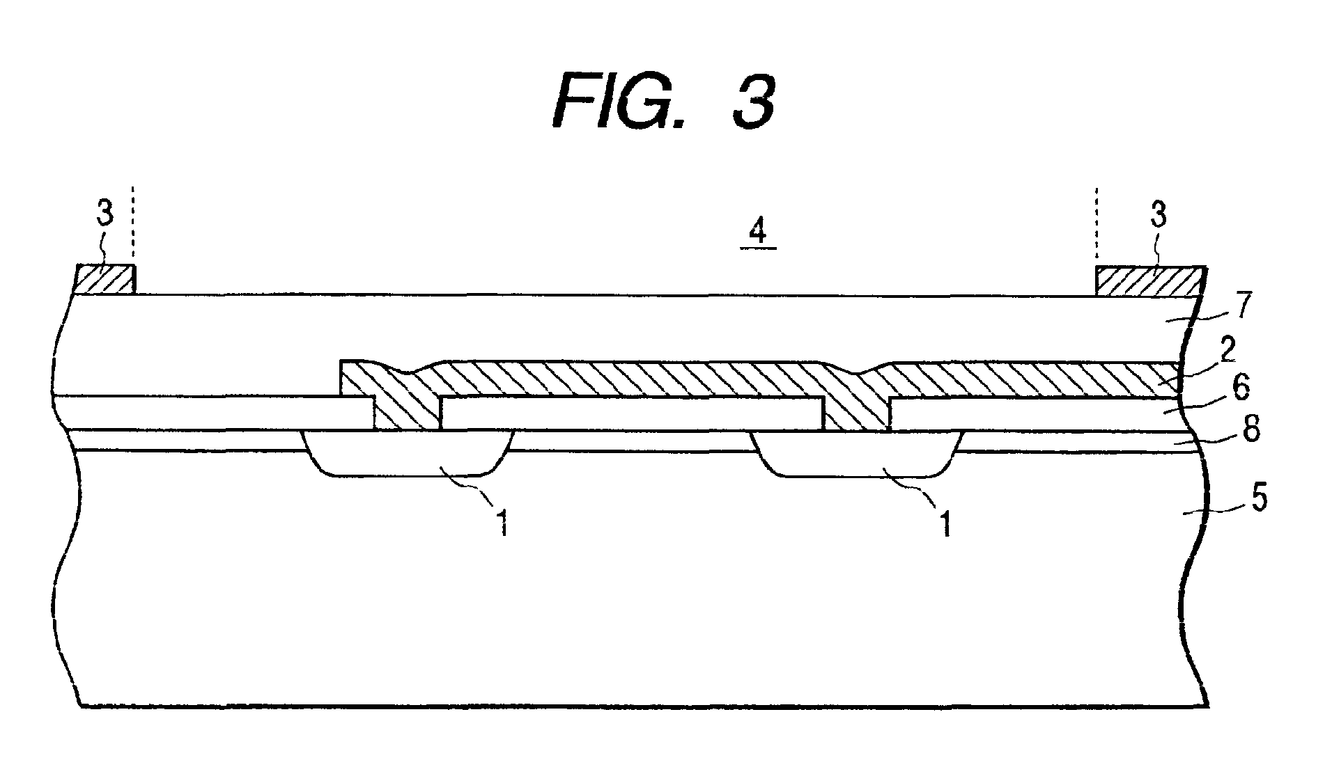
(57) There are provided a photoelectric conversion apparatus which comprises a light-receiving element including a semiconductor substrate (5) of a first conductivity type, a first semiconductor region (1) of a second conductivity type formed on the surface of the semiconductor substrate, transparent insulating layers (6,7) formed on the semiconductor substrate, and a light-shielding layer (3) formed on the insulating layer and having an opening (4) with an area larger than the first semiconductor region, and in which the light-receiving element includes a plurality of first semiconductor regions in a single opening, and the first semiconductor regions in the single opening are electrically connected to each other by interconnect (2), and an image sensor using the apparatus.


Search report