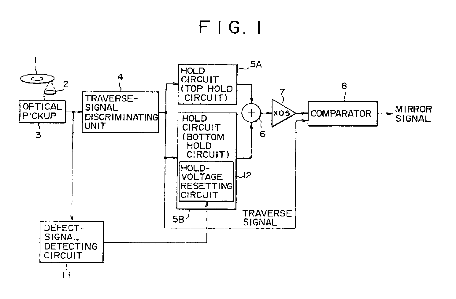
(57) When a signal is played back from a damaged portion of an optical disk, immediately
after the reproduction of the signal from the damaged portion, a mirror signal can
be obtained with a high degree of accuracy from conversion of a traverse signal into
a binary signal.
In a traverse-signal discriminating circuit, a traverse signal, a low-frequency component
of a playback signal, is separated from the playback signal and then supplied to a
hold circuit. In the hold circuit, the bottom of the traverse signal is held in order
to produce a bottom hold signal. In a defect detecting circuit, in the meantime a
defect in the playback signal, if any, is detected. If a defect is detected, the defect
detecting circuit outputs a defect signal at an H level to a hold-voltage resetting
circuit. The hold-voltage resetting circuit discharges a capacitor included in the
hold circuit, halting the operation to hold the bottom of the traverse signal as long
as the defect signal supplied thereto is set at the H level.
|
|
