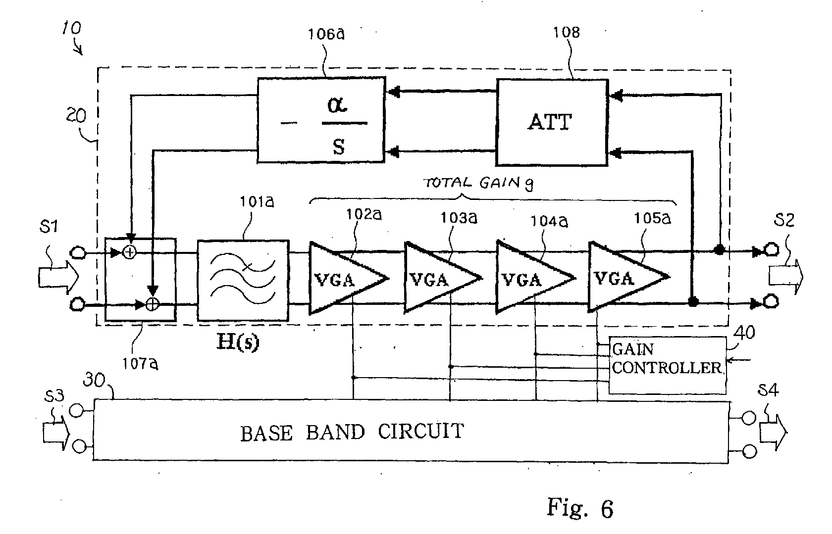
(57) A base band circuit (20) forms a part of an automatic gain controller (10) incorporated
in a direct conversion receiver, and includes a series of variable gain amplifiers
(102a/ 103a/ 104a/ 105a) controlled by a gain controller (40) and a feedback loop
(108/ 106a/ 107a) connected between the output node and the input node of the series
of variable gain amplifiers, wherein the feedback loop has an attenuation circuit
(108) connected between the output node of the series of variable gain amplifiers
and an inverted integrating circuit (106a) which, in turn, is connected through an
adder (107a) and a low pass filter (101a) to the input node of the series of variable
gain amplifiers so that direct current offset voltage is eliminated from the output
signal of the series of variable gain amplifiers without change of cut- off frequency.
|
|
