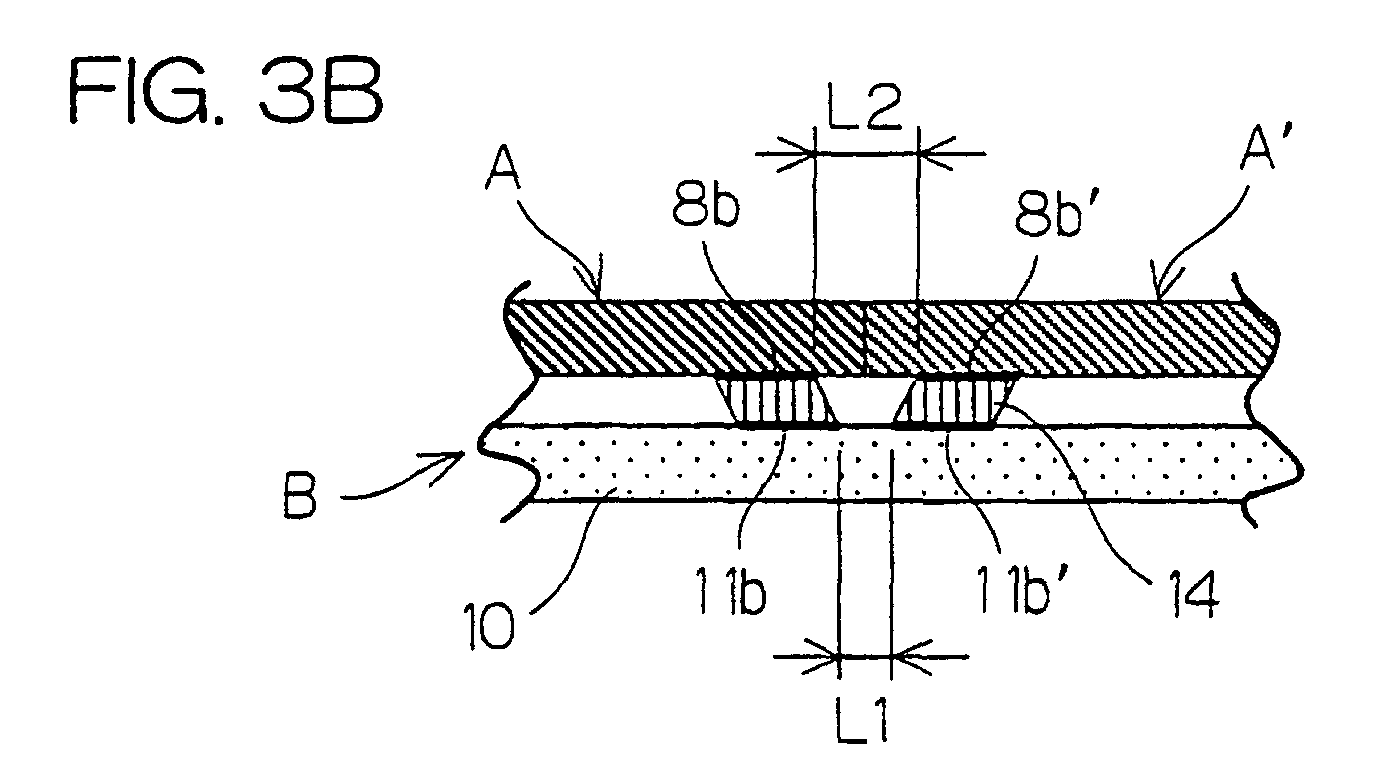
(57) A wiring board module has two wiring boards (A, A') placed on an external circuit
board (B). In each wiring board (A, A'), a terminal end of a laminated waveguide tube
(5) is exposed at a lateral side of a dielectric substrate (1), thus forming an. exposed
face (6), and the dielectric substrate (1) is provided at the bottom thereof in the
vicinity of the exposed face with connection pads (8a, 8b) to be used for mounting
the wiring board (A, A') on the surface of the external circuit board (B). The exposed
faces (6) of the laminated waveguide tubes (5, 5') of the two wiring boards (A, A')
are contacted with each other, and the connection pads (8a, 8b, 8a', 8b') at the bottoms
of the wiring boards (A, A') are connected and fixed to connection pads (11a, 11b,
11a', 11b') disposed on the surface of the external circuit board (B) (Fig. 3B).
|
|
