(19)
(11) EP 1 315 169 A3

(12) EUROPEAN PATENT APPLICATION

(88) Date of publication A3:
05.11.2003 Bulletin 2003/45

(43) Date of publication A2:
28.05.2003 Bulletin 2003/22

(21) Application number: 03003450.8

(22) Date of filing: 30.03.1999
(51) International Patent Classification (IPC)7G11C 5/14
(84) Designated Contracting States:
DE FR GB NL SE

(30) Priority: 31.03.1998 JP 8661598

(62) Application number of the earlier application in accordance with Art. 76 EPC:
99106473.4 / 0947990

(71) Applicant: NEC CORPORATION
Tokyo (JP)

(72) Inventor:
  • Miki, Atsunori
    Minato-ku, Tokyo (JP)

(74) Representative: Betten & Resch 
Postfach 10 02 51
80076 München
80076 München (DE)


(54) Booster circuit for semiconductor device


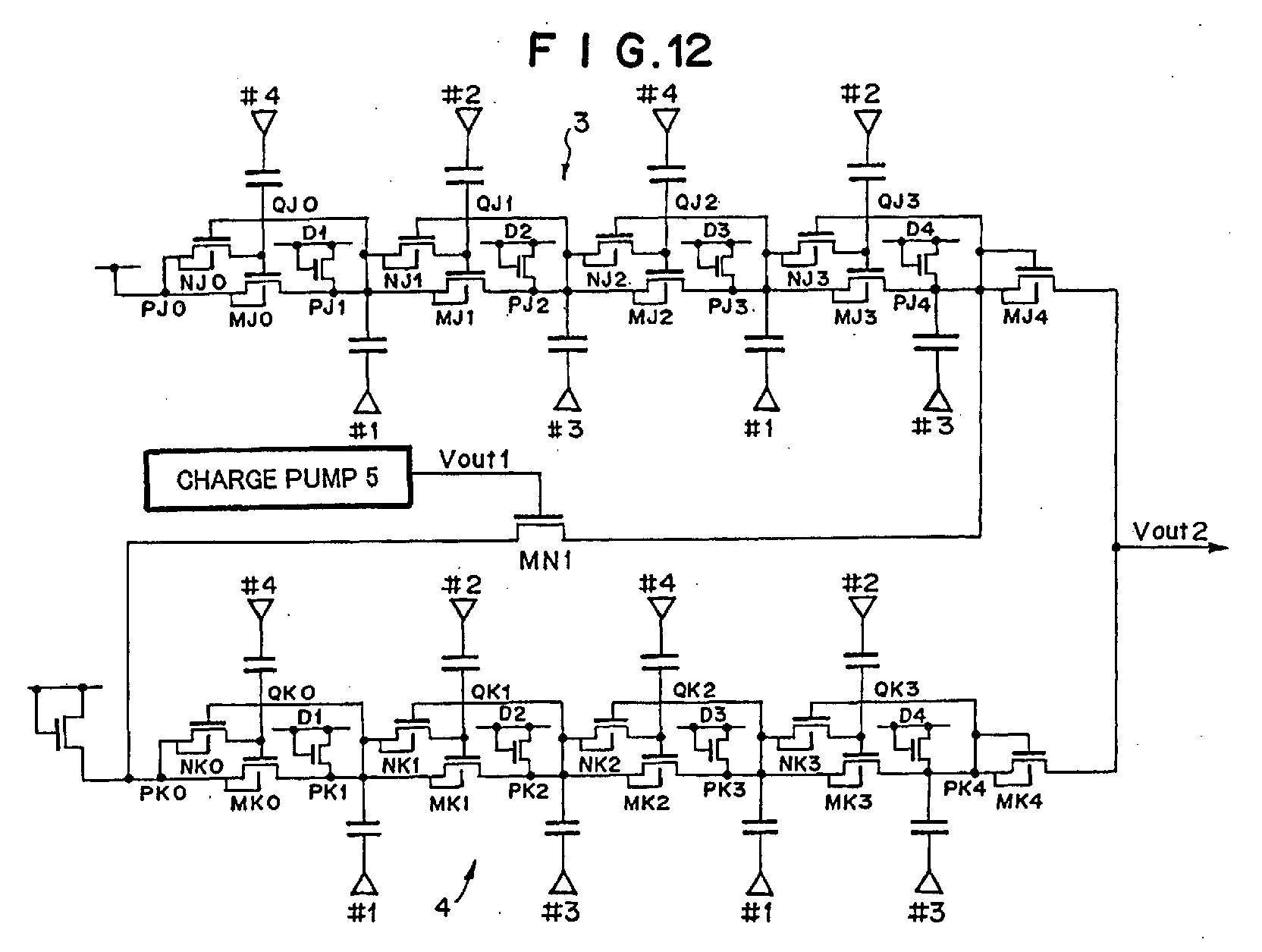
(57) A booster circuit is disclosed, the booster circuit having at least three charge pumps, each of the charge pumps having at least one booster cell for boosting a voltage, wherein a transistor is disposed in such a manner that an output terminal of a first charge pump is connected to a drain of the transistor, an input terminal of a second charge pump is connected to a source of the transistor, an output terminal of a third charge pump is connected to a gate of the transistor, and the output terminal of the first charge pump is connected to an output terminal of the second charge pump.


Search report