|
(11) | EP 1 424 773 A1 |

| (12) | EUROPEAN PATENT APPLICATION |
|
|
|
|
||||||||||||||||||||
| (54) | Circuit device for realising a non-linear reactive elements scale network |
| (57) The invention relates to a circuit device (1) for realising a non-linear reactive
elements scale network, wherein the non-linear elements of the network are pairs of
inductive (L) and capacitive (C) components cascade connected between a pair of input
terminals and a pair of output terminals. Advantageously in the invention, each component
(L,C) of the network is formed by cascade connecting a first (2) and a second (3)
transconductance (Gm1,Gm2) integrator with each other. |
Field of Application
[0001] The present invention relates to a circuit device for realising a non-linear reactive elements scale network.
[0002] More particularly, the invention relates to a circuit device for realising non-linear reactive elements scale network, wherein the non-linear elements in the network are pairs of inductive and capacitive components cascade connected between a pair of input terminals and a pair of output terminals.
[0003] The invention applies specifically to read-channel devices for hard disk drivers (HDDs), and broadly to digital communication systems, being part of a substitutive architecture of the so-called "partial-maximum likelihood response" (PRML) systems. This because it is considered that a "non-linear channel", based on the scale network as above, can provide stronger information decoding as for noise if compared to a standard scale (e.g., PRML, Peak Detection, etc.).
Prior Art
[0004] As it is well known in this technical field, for applications relating to non-linear decoding channels for digital transmission, electronic devices capable of implementing a scale network comprising LC non-linear elements would be needed. In fact, research carried out by the Applicant indicates that a non-linear channel would provide improved performance with respect to a standard transmission channel.
[0005] For example, the here-attached Figure 1 schematically illustrates the structure of a scale network comprising n LC non-linear elements cascade connected together.
[0006] The network of Figure 1 is essentially a quadrupole having a pair of input terminals to which a voltage potential Vo is applied, and having a pair of output terminals to which a resistive load Rt is connected.
[0007] All the pairs of LC non-linear elements, which is L1, C1;..., Li, Ci,...,Ln, Cn, have the same value. In other words, all the L components are identical with one another, as are the C components.
[0008] In particular, the non-linear relations that the network of Figure 1 would be expected to implement are the following:
Relation (1)
where, Co and Vo are constants; and
Relation (2)
where, L0 and I0 are constants.
[0010] A bipolar transistor differential cell BJT receives a bias current I1 on a first circuit branch, and it is connected to ground by a current generator I. A potential equal to Vc lies across the emitter terminals of the transistor pair.
[0011] A transistor output stage, being supplied by a current Ic, is connected to said first circuit branch and has an output terminal connected to ground through the parallel of a capacitance and a current generator.
[0013] The exponential voltage-current characteristic of the transistor pair BJT of the differential cell allows the desired non-linear relations to be sinthesized where the substitution indicated in Relation (3) is carried into effect.
[0014] However, the dynamic performance of this hypothetical embodiment based on the use of a derivator would be inadequate to meet the requirements of the above application field.
[0015] If taking into consideration the non-linear capacitance alone, a possible embodiment of the network of Figure 1 could be provided through the use of an integrator instead of a derivator. In this way, the superior dynamic characteristics of the integrator with respect to the derivator could be exploited.
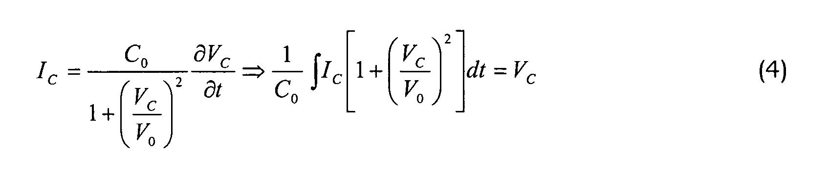
[0016] An embodiment baesd on an integrator should implement the following operations:
Relation (4)
[0017] A circuit device realised according to Relation (3) would be highly complicated. Moreover this would be even worse since the scale network of Figure 1 contains n LC pairs and, when the number n is greater than 10, as required in most applications, the complexity of the circuit embodiment would limit high-frequency performance.
[0018] The underlying technical problem of this invention is to provide a circuit device for realising a non-linear reactive elements network, which device has suitable structural and functional features for the network to be implemented by minimizing complexity occupied area, and this without employing integrated inductors.
Summary of the Invention
[0019] The solving idea on which this invention is based is that of implementing the scale network by using transconductance integrators but simulating non-linear inductors.
[0020] On the basis of the above idea, the technical problem is solved by a device as previously indicated and as defined in the characterizing part of Claim 1 herewith enclosed.
[0021] The features and advantages of the device according to the invention will become apparent from the following description of an embodiment thereof, given by way of non-limitative example with reference to the accompanying drawings.
Brief Description of the Drawings
[0022]
Figure 1 shows schematically a scale network comprising n LC non-linear elements.
Figure 2 shows schematically a conventional circuit based on a derivator for implementing the scale network of Figure 1.
Figure 3 shows schematically a circuit device according to this invention.
Figure 4 is schematical view of the circuit detail of the device in Figure 3.
Figure 5 shows schematically a portion of the scale network according to this invention realised by means of several devices of Figure 3.
Detailed Description
[0023] With reference to the drawings, in particular to the embodiments illustrated by Figures 3 and 4, 1 generally end schematically show a circuit device according to the invention for implementing a network 5 of reactive LC non-linear elements, e.g. a network as shown schematically in Figure 1.
[0024] The device 1 has a pair of input terminals A, B on which differential input voltages Vin+ and Vin-, are respectively applied.
[0025] The device 1 also has a pair of output terminals O1, O2 where differential output voltages Vout+ and Vout- are respectively produced.
[0027] The differential output pair U1, U2 of this first integrator Gm1 are connected each to a respective differential input A2, B2 of a second transconductance (Gm2) integrator 3.
[0028] In a preferred embodiment, the transconductance Gm1 of the first integrator 2 has the same value as the transconductance Gm2 of the second integrator 3.
[0030] The second integrator 3 has differential outputs that are coincident with the outputs O1 and O2 of the device 1.
[0031] These outputs O1 and O2 are coupled to a feedback CMFB (Common Mode FeedBack) block 4 arranged to provide a reference signal CMFB_ref for the bias circuit portion of the second integrator 3.
[0032] The outputs O1, O2 of the device 1 are further coupled to ground through respective stabilization capacitance Co.
[0033] Briefly, the differential input voltage Vin+, Vin- corresponds to current Ic of Relation (4), and the differential output voltage Vout+, Vout-corresponds to voltage Vc of the same Relation (4).
[0034] The integrator pair 2 and 3 basically simulate the frequency performance of a capacitance C in the scale network of Figure 1.
[0035] Also the non-linear inductor L may be implemented through an identical integrator pair design.
[0036] In the latter case, the differential input voltage Vin+, Vin- corresponds to voltage V1 of the inductor, and the differential output voltage Vout+, Vout- corresponds to current I1.
[0037] The device 1 of this invention has, therefore, no integrated inductors, so that the circuit complexity and overall occupied area of the device can be minimized.
[0039] It should be understood that both the first 2 and the second 3 integrator are formed with mixed bipolar-MOS technology by means of bipolar transistor differential cells biased by MOS circuit portions.
[0040] The first integrator 2 comprises a differential cell having a double pair of transistors, Q1, Q2 and Q3, Q4, which is associated with the differential inputs A, and B.
[0041] A bias circuit portion, comprising MOS transistors M1,..., M6, is arranged to couple the differential cell with the supply voltage references Vdd and the bias voltage and current references I1 and V1.
[0042] The transistors Q5, Q6 and Q7, diode configurated, couple the outputs U1, U2 of the first integrator 2 to ground.
[0043] The outputs U1, U2 of the integrator 2 are connected to the respective inputs A2, B2 of the second integrator 3, the latter showing a differential cell structure of bipolar transistors with a double pair of input transistors Q8, Q9 and Q10, Q11.
[0044] A bias circuit portion comprised of MOS transistors M7, M8, M9 and M10 couples the differential cell of integrator 3.
[0045] A feedback block 4 connects the outputs O1, O2 of the second integrator 3 to the bias circuit portion in order to provide a voltage reference CMFB_ref for the transistor pair M7, M9.
[0047] As said before, the device 1 allows the performance of one of the non-linear components of the scale network of Figure 1, both the capacitive component C and the inductive component L, to be emulated.
[0048] Thus, the scale network structure can be reconstructed by using a plurality of suitably interconnected devices 1.
[0049] Shown in Figure 5 is an exemplary portion of a scale network realised by connecting several devices 1 together, which are similar to the device described hereinabove.
[0050] Figure 5 shows a first device 1, emulating a first inductor L1, as being connected to the voltage generator Vo at the first differential input A.
[0051] The output O1 is connected to ground, and the output O2 is connected to the differential input A of a second device 1 emulating the capacitor C1.
[0052] The output O2 of the second device emulating C1, is connected to the differential input B of the first device emulating L1.
[0053] The output O1 of the second emulating C1, is connected to the differential input A of a third device 1 emulating a second inductor L2 in the scale network.
[0054] The output O1 of the third device emulating L2 is connected to the differential input B of the second device emulating C1, and so on.
[0055] In this way, a non-linear scale network can be implemented with at least twenty LC elements, without using integrated inductors.
[0056] The network implemented with a cascade of devices 1 according to the invention has shown to have excellent characteristics of frequency response.
1. A circuit device (1) for realising a non-linear reactive elements scale network, wherein
the non-linear elements of the network are pairs of inductive (L) and capacitive (C)
components cascade connected between a pair of input terminals and a pair of output
terminals, characterised in that each component (L,C) of the network is formed by cascade connecting a first (2) and
a second (3) transconductance (Gm1,Gm2) integrator with each other.
2. A device according to Claim 1, characterised in that each integrator comprises a bipolar transistor input circuit portion and a MOS transistor
bias circuit portion, and that the outputs of the second integrator (3) are feedback
connected to the bias circuit portion of the same integrator through a feedback block
(4).
3. A device according to Claim 2, characterised in that said feedback block (4) provides a voltage reference (CMFB_ref) for said bias circuit
portion.
4. A device according to Claim 1, characterised in that the outputs (U1,U2) of the first integrator (2) connected to the inputs (A2,B2) of
the second integrator (3) are further coupled to ground by respective diodes (Q5,Q6).
5. A device according to Claim 1, characterised in that it comprises differential outputs (O1,O2) respectively coupled to ground through
a stabilization capacitance (Co).
6. A device according to Claim 1, characterised in that the first (2) and the second (3) integrator have the same transconductance (Gm1,Gm2).
7. A device according to Claim 1, characterised in that each pair of integrators (2,3) implements the following relation, in order to emulate
a capacitor (C), or a similar relation with L indexes in order to emulate an inductor
(L):
8. A scale network (5) of LC non-linear elements, characterised in that it comprises at least twenty devices (1) as claimed in Claim 1.