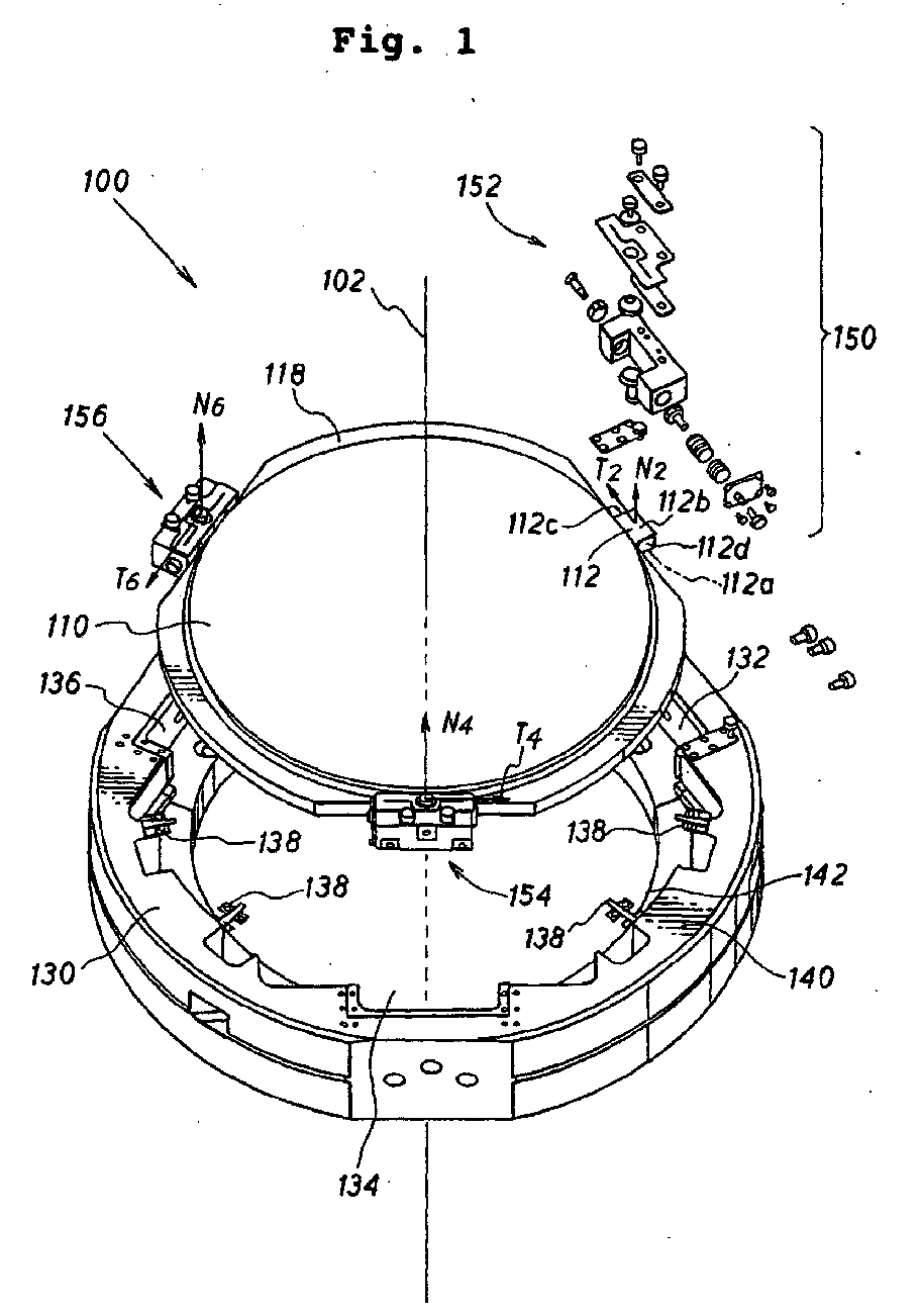
(57) An optical mounting assembly, such as a lens cell assembly, method for making a lens
cell assembly, and method for supporting a lens in the lens cell assembly are provided
to kinematically mount an optical element to an optical holder. The optical mounting
assembly includes an optical element (110) having a plurality of mounting pads (112)
distributed around an outer circumference of the optical element, and an optical holder
having a corresponding plurality of clamping brackets (150) distributed around an
inner circumference of the optical holder. The optical holder supports or constrains
movement of the optical element at points of contact between the plurality of mounting
pads and the corresponding plurality of clamping brackets both in a normal direction
parallel to the optical axis (102) of the assembly and in a tangential direction of
the corresponding mounting pad. When the optical element has three mounting pads and
the optical holder constrains the optical element at corresponding three clamping
brackets, the optical element is constrained in six degrees of freedom, three in the
normal direction and another three in the tangential direction at the corresponding
mounting pads. The optical mounting assembly of this invention can be used in combination
with a projection lens assembly in a semiconductor wafer manufacturing process.
|
|
