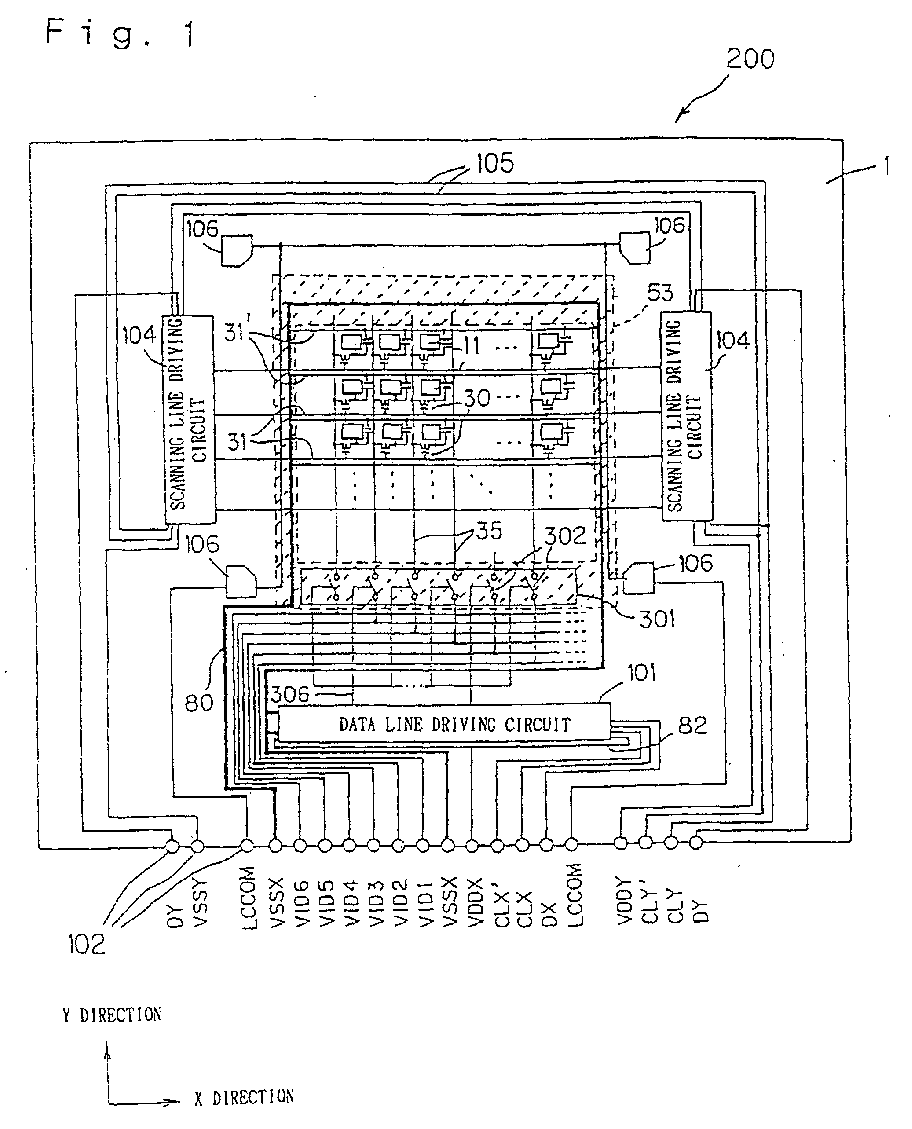
(57) An electrooptical apparatus comprising a substrate (1) and elements formed on said
substrate (1), said elements including: a plurality of scanning lines (31); a plurality
of data lines (35) crossing said plurality of scanning lines (31); a plurality of
switching elements (30) disposed in correspondence with intersections between said
plurality of scanning lines (31) and said data lines (35); a plurality of pixel electrodes
(11) disposed in correspondence with said plurality of switching elements (30); data
signal supply means (101, 104, 301) for supplying, in response to a clock signal,
a data signal corresponding to an image signal to said plurality of data lines (35);
an image signal line (VID1-VID12) for supplying said image signal input via an image
external input terminal to said data signal supply means (101, 104, 301); a clock
signal line (CLX, CLX') for supplying said clock signal input via a clock external
input terminal to said data signal supply means (101, 104, 301); and an electrically
conductive line (84) maintained at a constant electric potential for shielding said
image signal line (VID1-VID12) from said clock signal line (CLX,CLX'), wherein said
electrically conductive line (84) includes a part made up of a constant electric potential
line for supplying a constant electric potential power-supply to said data signal
supply means (101, 104, 301); characterised in that the part of said electrically
conductive line (84) substantially surrounds said clock signal line (CLX, CLX') on
said substrate so as to electrically shield the clock signal line (CLX, CLX').
|
|
