(19)
(11) EP 1 308 946 A3

(12) EUROPEAN PATENT APPLICATION

(88) Date of publication A3:
13.10.2004 Bulletin 2004/42

(43) Date of publication A2:
07.05.2003 Bulletin 2003/19

(21) Application number: 02257519.5

(22) Date of filing: 30.10.2002
(51) International Patent Classification (IPC)7G11B 11/08, G11B 11/12, G11B 9/04, G11B 9/10
(84) Designated Contracting States:
AT BE BG CH CY CZ DE DK EE ES FI FR GB GR IE IT LI LU MC NL PT SE SK TR
Designated Extension States:
AL LT LV MK RO SI

(30) Priority: 30.10.2001 US 984419

(71) Applicant: Hewlett-Packard Company
Palo Alto, CA 94304 (US)

(72) Inventor:
  • Gibson, Gary A.
    Palo Alto, CA 94301 (US)

(74) Representative: Jehan, Robert et al
Williams Powell Morley House 26-30 Holborn Viaduct
London EC1A 2BP
London EC1A 2BP (GB)


(54) Data storage device


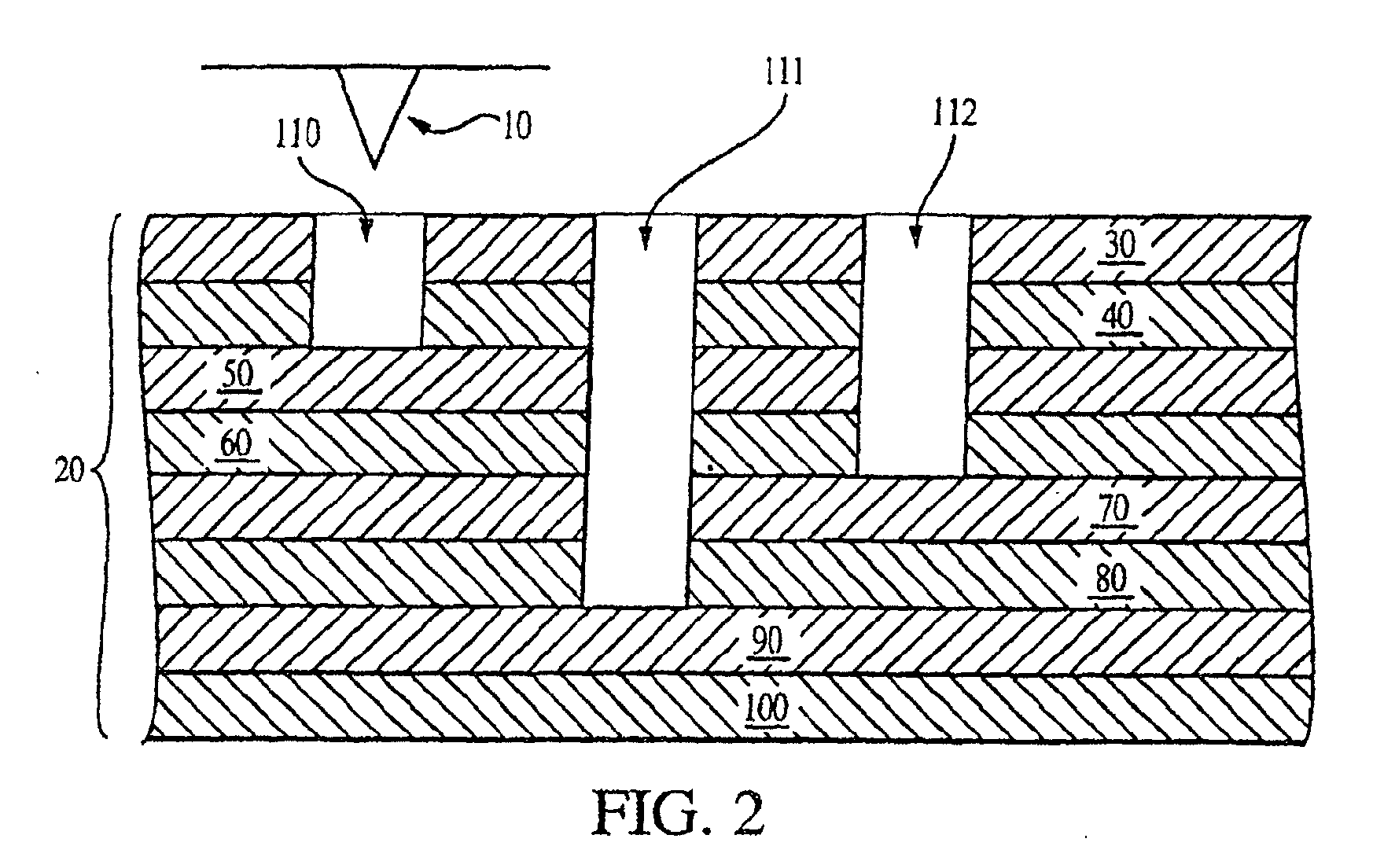
(57) A data storage medium (20) includes several stacked layers (30,40,50,60,70,80,90,140,160,180) which can be conducting, insulating, resistive, or capable of changing between two or more states or phases. A data storage device includes the data storage medium (20) and an energy source (10) that can form nanometer-scaled data bits (110,111,112,113,150) in regions of the data storage medium (20). The data bits (110,111,112,113,150) can include holes through some of the stacked layers (30,40,50,60,70,80,90,140,160,180) or phase changes in portions of the layers capable of changing between two or more states. Method of using such a storage medium (20) to store nanometer scaled data bits (110,111,112,113,150).


Search report