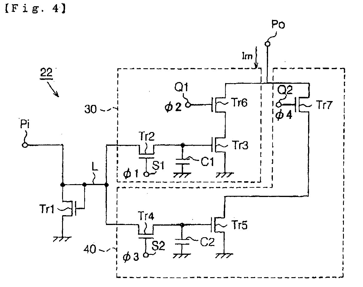
(57) The invention seeks to provide an electronic circuit, an electronic device and an
electronic apparatus, which are capable of forming a simple circuit for supplying
data signals to an electro-optical pixel element of a display. A first buffer circuit
(30) is formed of second, third and sixth transistors (Tr2,Tr3,Tr6) and a first capacitor
(C1). A second buffer circuit (40) is formed of fourth, fifth and seventh transistors
(Tr4,Tr5,Tr7) and a second capacitor (C2). The drain of the second transistor (Tr2)
of the first buffer circuit (30) and the drain of the fourth transistor (Tr4) of the
second buffer circuit (40) are connected to the first transistor (Tr1). Furthermore,
the drain of the sixth transistor (Tr6) of the first buffer circuit (30) is connected
to the drain of the seventh transistor (Tr7) of the second buffer circuit (40) through
an analog output terminal (Po). Thus when one of the first and second buffer circuits
performs output to a data line (Po), the other of the two buffers receive an input
signal (Pi).
|
|
