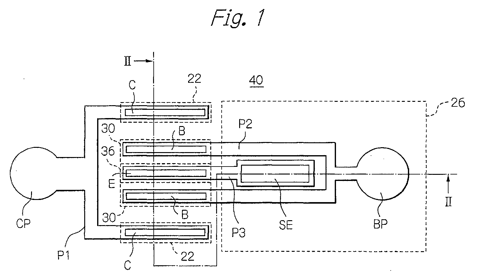
(57) A semiconductor device includes a low resistance semiconductor substrate (10), a
high resistance semiconductor layer (12, 16) formed on the substrate, an insulation
layer (28, 38, 40) formed on the semiconductor layer, and a transistor element composed
of a collector region (14), a base region (18), and an emitter region (20) formed
in the semiconductor layer. The device further includes an emitter electrode (E) formed
in the insulation layer to be connected to the emitter region, a sub-emitter electrode
(SE) formed in the insulation layer connected to the emitter electrode, a low resistance
impurity-diffusion region formed in the semiconductor layer such that the sub-emitter
electrode is connected to the substrate through the impurity-diffusion region, a base
electrode (B) formed in the insulation layer to be connected to the base region, and
a base-bonding pad (BP) formed on the insulation layer to be connected to the base
electrode. The base-bonding pad is placed on the insulation layer above the impurity-diffusion
region to be at least partially encompassed with the impurity-diffusion region.
|
|
