(19)
(11) EP 1 271 598 A3

(12) EUROPEAN PATENT APPLICATION

(88) Date of publication A3:
26.10.2005 Bulletin 2005/43

(43) Date of publication A2:
02.01.2003 Bulletin 2003/01

(21) Application number: 02090223.5

(22) Date of filing: 25.06.2002
(51) International Patent Classification (IPC)7H01J 17/04, H01J 17/49, H01J 9/02
(84) Designated Contracting States:
AT BE CH CY DE DK ES FI FR GB GR IE IT LI LU MC NL PT SE TR
Designated Extension States:
AL LT LV MK RO SI

(30) Priority: 25.06.2001 JP 2001191765

(71) Applicant: Pioneer Corporation
Meguro-ku Tokyo (JP)

(72) Inventors:
  • Okigawa, Akifumi
    Minato-ku, Tokyo (JP)
  • Yoshioka, Toshihiro
    Minato-ku, Tokyo (JP)

(74) Representative: Betten & Resch 
Patentanwälte Postfach 10 02 51
80076 München
80076 München (DE)


(54) Plasma display panel and method of manufacturing the same


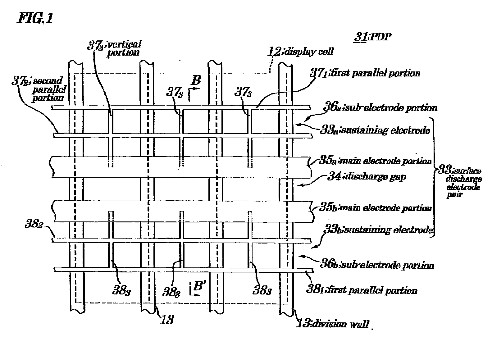
(57) A plasma display panel (31) having a plurality of surface discharge electrode pairs (33) formed in a column direction at predetermined intervals, each surface discharge electrode pair (33) having a pair of sustaining electrodes (33a,33b) extending in a row direction so that a discharge gap (34) is put between the sustaining electrodes (33a,33b). Each sustaining electrode (33a,33b) is provided with a main electrode portion (35a,35b) made up of a transparent conductive thin film formed in stripe shapes so as to face the discharge gap (34) and a sub-electrode portion (36a,36b) made up of a metal film of narrow width formed at a side opposite to the discharge gap (34) side of the main electrode portion (35a,35b) to which it corresponds. With this configuration, a high image quality and a low power consumption can be obtained.


Search report