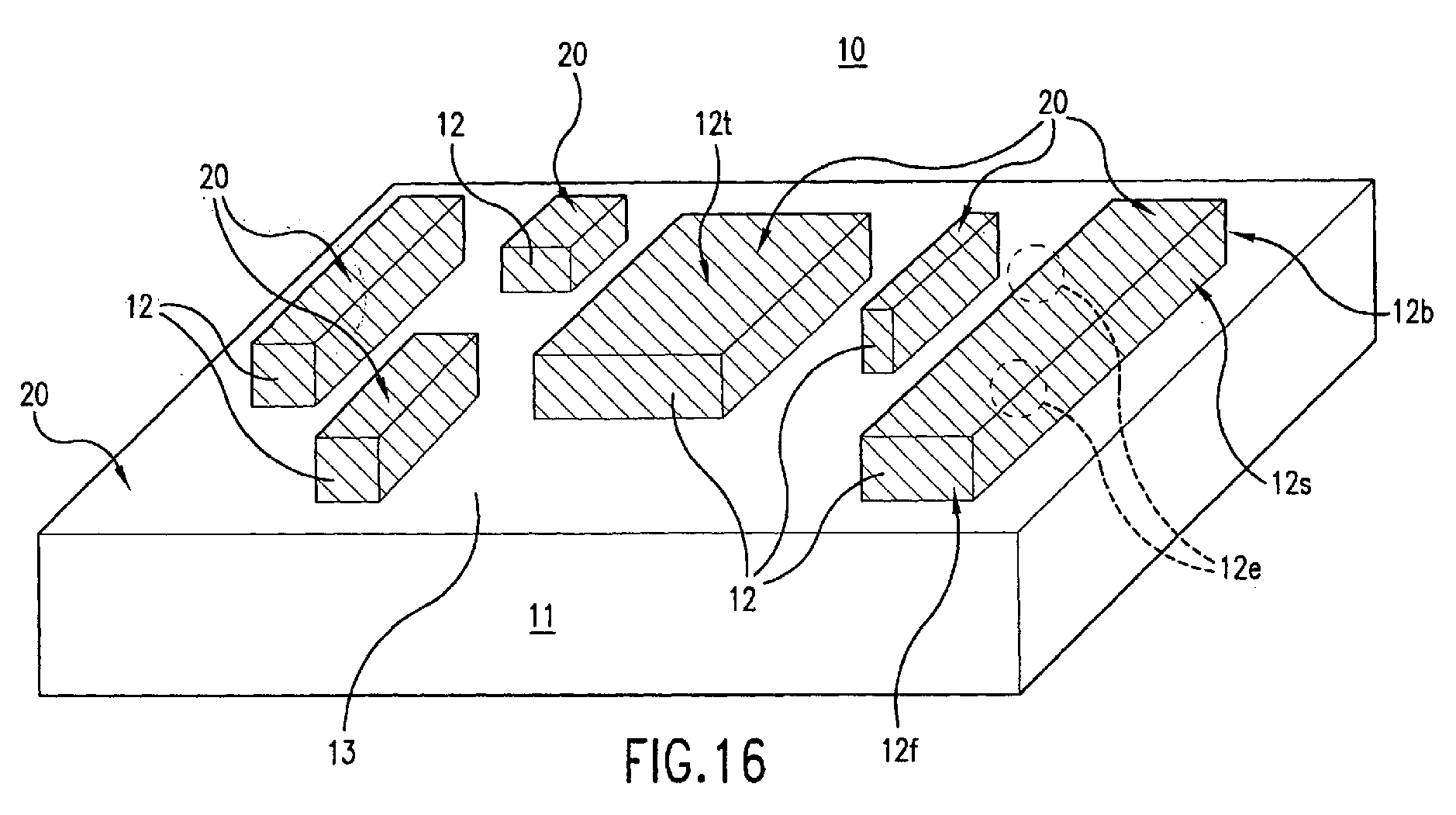
(57) A hardened nano-imprinting stamp (10) includes a plurality of silicon-based nano-sized
features (12) that have a hardened shell (20) of silicon carbide, silicon nitride,
or silicon carbide nitride. The hardened shell (20) is made harder than the underlying
silicon by a plasma carburization and/or a plasma nitridation process. During the
plasma process, atoms of carbon C and/or nitrogen N bombard and penetrate a plurality
of exposed surfaces (12e, 12s, 12t, 12b, 12f, 13) of the nano-sized features 12 and
chemically react with the silicon (Si) to form the hardened shell (20) of silicon
carbide, silicon nitride, or silicon carbide nitride. The lifetime, durability, economy,
and accuracy of the resulting hardened nano-imprinting stamp (10) are improved.
|
|
