(19)
(11) EP 1 467 376 A3

(12) EUROPEAN PATENT APPLICATION

(88) Date of publication A3:
08.02.2006 Bulletin 2006/06

(43) Date of publication A2:
13.10.2004 Bulletin 2004/42

(21) Application number: 04252124.5

(22) Date of filing: 08.04.2004
(51) International Patent Classification (IPC): 
G11C 11/16(2006.01)
H01L 27/115(2006.01)
G11C 11/22(2006.01)
H01L 27/22(2006.01)
(84) Designated Contracting States:
AT BE BG CH CY CZ DE DK EE ES FI FR GB GR HU IE IT LI LU MC NL PL PT RO SE SI SK TR
Designated Extension States:
AL HR LT LV MK

(30) Priority: 11.04.2003 JP 2003108021

(71) Applicant: SHARP KABUSHIKI KAISHA
Osaka 545-8522 (JP)

(72) Inventor:
  • Morimoto, Hidenori
    Kashihara-shi, Nara 634-0077 (JP)

(74) Representative: Brown, Kenneth Richard et al
R.G.C. Jenkins & Co. 26 Caxton Street
London SW1H 0RJ
London SW1H 0RJ (GB)


(54) Memory cell, memory device and manufacturing method of memory cell


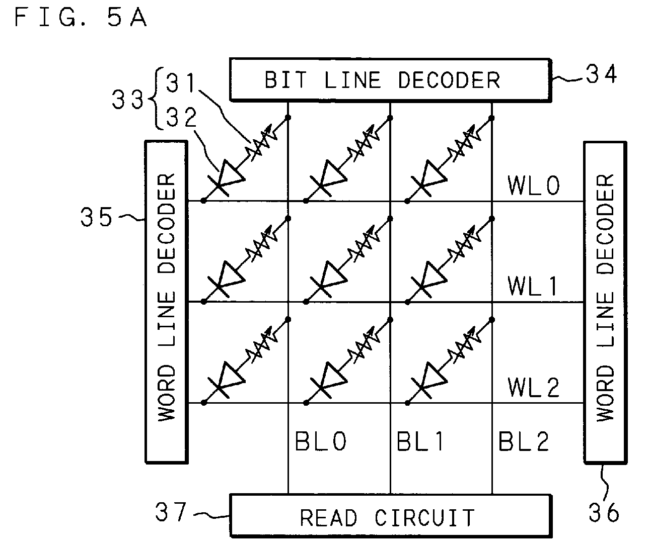
(57) A memory cell (33) in which a variable resistive element (31) and a Schottky diode (32) are connected in series to each other. In a memory device, bit lines (BL0, BL1 and BL2) are arranged in a column direction, one end of the bit line (BL) is connected to a bit line decoder (34), and the other end thereof is connected to a reading circuit (37). Word lines (WL0, WL1 and WL2) are arranged in a row direction so as to intersect with the bit lines (BL), and both ends of the word line (WL) are connected to word line decoders (35 and 36). In other words, the bit line (BL) and the word line (WL) are arranged in a matrix and a memory cell (33) is located at a position where the bit line (BL) and the word line (WL) intersect with each other, which constitutes the memory device. An influence of a reading disturbance in the memory cell (33) and the memory device is reduced.


Search report