(19)
(11) EP 1 478 215 A3

(12) EUROPEAN PATENT APPLICATION

(88) Date of publication A3:
08.02.2006 Bulletin 2006/06

(43) Date of publication A2:
17.11.2004 Bulletin 2004/47

(21) Application number: 04394023.8

(22) Date of filing: 07.05.2004
(51) International Patent Classification (IPC): 
H05K 3/30(2006.01)
H05K 3/46(2006.01)
(84) Designated Contracting States:
AT BE BG CH CY CZ DE DK EE ES FI FR GB GR HU IE IT LI LU MC NL PL PT RO SE SI SK TR
Designated Extension States:
AL HR LT LV MK

(30) Priority: 14.05.2003 US 437006

(71) Applicant: Nortel Networks Limited
St.Laurent, Quebec H4S 2A9 (CA)

(72) Inventors:
  • Difilippo, Luigi
    Kanata, ON K2T 1C7 (CA)
  • Wyrzykowska, Aneta
    Kanata, ON K2L 3N2 (CA)
  • Kwong, Herman
    Kanata, ON K2L 3S2 (CA)

(74) Representative: Boyce, Conor et al
F.R. Kelly & Co, 27 Clyde Road
Ballsbridge, Dublin 4
Ballsbridge, Dublin 4 (IE)


(54) Package modification for channel-routed circuit boards


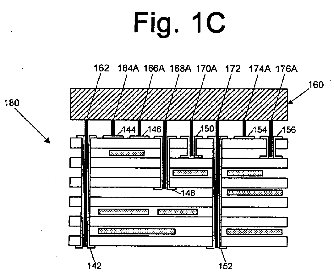
(57) A method for implementing a circuit component (160) on a surface of a multilayer circuit board (110) is provided. The circuit component includes a plurality of pins (162,164,166,168,170,172,174,176) and the circuit board (110) includes a plurality of electrically conductive vias (142,148,150,152,156) penetrating at least one layer of the circuit board (110) and being arranged so as to form at least one channel for routing one or more traces at one or more signal layers of the circuit board (110). The method comprises the step of forming at least one pin (162,168A,170A,172,176A) of the plurality of pins (162,164,166,168,170,172,174,176) of the circuit component (160) to have a length compatible with a depth of a corresponding via (142,148,150,152,156) of the circuit board (110).


Search report