(57) An optical multilayer structure (1) has a transparent substrate, a transparent first
layer (11) in contact with the substrate (10), a gap portion (12) having a changeable
size capable of causing an optical interference phenomenon, and a transparent second
layer (13). By changing the size of the gap portion (12), an amount of reflection,
transmission, or absorption of incident light can be changed. Also in a visible light
area, high response is realized. Consequently, the optical multilayer structure can
be suitably used for an image display.
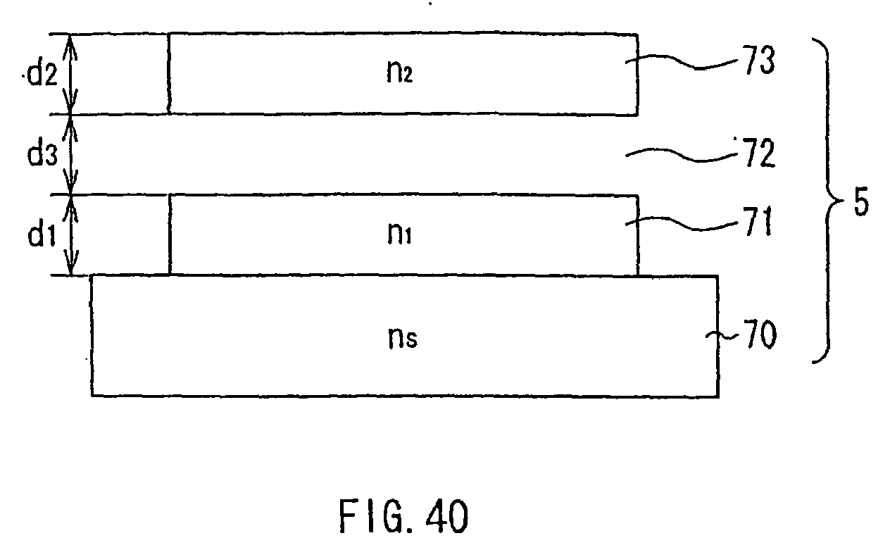
In one alternative the optical multilayer structure may be obtained by stacking, on
a substrate, a first transparent layer made of a material having a high refractive
index such as TiO2 (n = 2.40), a second transparent layer made of a material having a low refractive
index such as MgF2 (n = 1.38), a gap portion having a changeable size capable of causing an optical
interference phenomenon, and a third transparent layer made of a material having a
high refractive index such as TiO2.
The structure may be used in an optical switching device and in an image display.
|
|
