(19)
(11) EP 2 056 301 A3

(12) EUROPEAN PATENT APPLICATION

(88) Date of publication A3:
17.06.2009 Bulletin 2009/25

(43) Date of publication A2:
06.05.2009 Bulletin 2009/19

(21) Application number: 09151003.2

(22) Date of filing: 29.06.2001
(51) International Patent Classification (IPC): 
G11C 11/406(2006.01)
G11C 7/22(2006.01)
(84) Designated Contracting States:
AT BE CH CY DE DK ES FI FR GB GR IE IT LI LU MC NL PT SE TR

(30) Priority: 07.07.2000 CA 2313954
07.07.2000 US 216679

(62) Application number of the earlier application in accordance with Art. 76 EPC:
01949156.2 / 1307884

(71) Applicant: Mosaid Technologies Incorporated
Kanata, ON K2K 2X1 (CA)

(72) Inventor:
  • Demone, Paul
    Kanata, Ontario K2L 4B7 (CA)

(74) Representative: Borsano, Corrado et al
Notarbartolo & Gervasi S.p.A. Corso di Porta Vittoria, 9
20122 Milano
20122 Milano (IT)


(54) A high speed dram architecture with uniform access latency


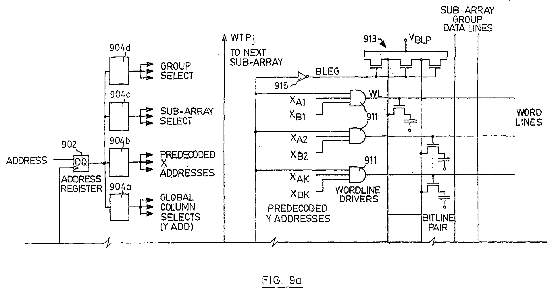
(57) A Dynamic Random Access Memory (DRAM) performs read, write, and refresh operations. The DRAM includes a plurality of sub-arrays, each having a plurality of memory cells, each of which is coupled with a complementary bit line pair and a word line. The DRAM further includes a word line enable device for asserting a selected one of the word lines and a column select device for asserting a selected one of the bit line pairs. A timing circuit is provided for controlling the word line enable device, the column select device, and the read, write, and refresh operations in response to a word line timing pulse. The read, write, and refresh operation are performed in the same amount of time.


Search report