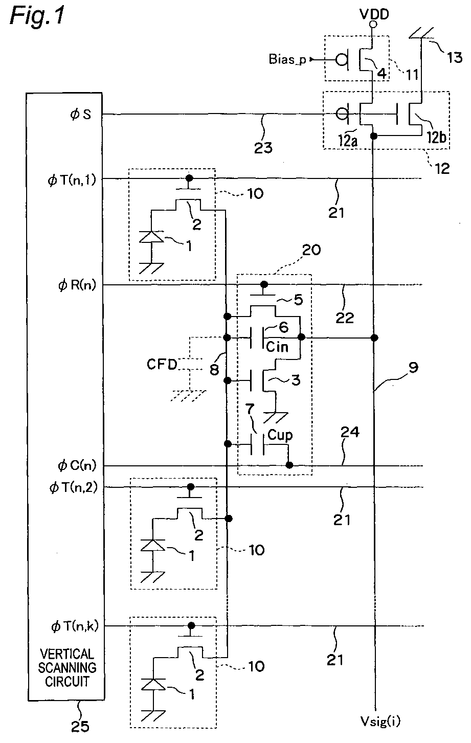
(57) In the amplification type solid-state imaging device of the present invention, the
input side of a switched capacitor amplifier portion 20 is connected to the output
side of each transfer transistor 2 of a photoelectric conversion and transfer portion
group obtained by grouping a plurality of photoelectric conversion and transfer portions
10 having a photodiode 1 and a transfer transistor 2, and the output side of the switched
capacitor amplifier portion 20 is connected to a vertical signal line 9. The switched
capacitor amplifier portion 20 has a signal charge storage portion 8, an amplification
transistor 3 whose input side is connected to the signal charge storage portion 8,
and a capacitor 6 and a reset transistor 5 connected between the input and output
of the amplification transistor 3. By controlling the reset transistor 5 and a switchover
portion 12 by a control section 25, the input side voltage of the inverting amplifier
constructed of the amplification transistor 3 and the constant current load transistor
4 is controlled. According to the device, a high-quantity image can be obtained, and
the pixel size can be reduced.
|
|
