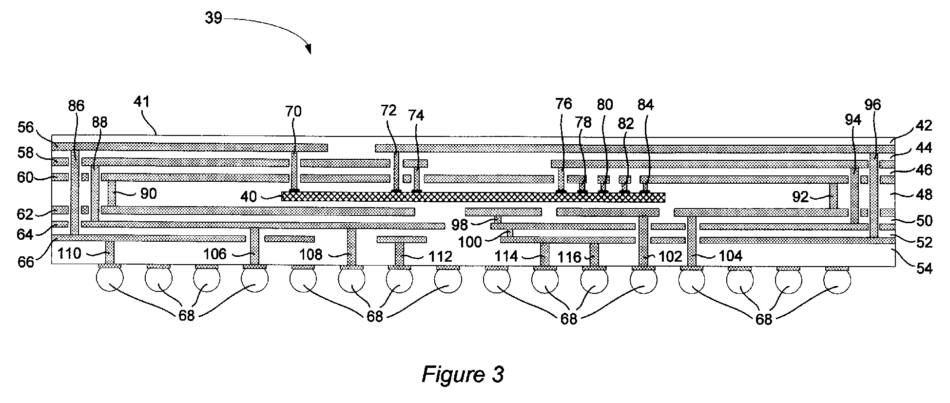
(57) A semiconductor package (39) comprises a combination die (40) embedded in a base
(41). The combination die (40) comprises a plurality of functional blocks (24,30,36),
where the functional blocks are insulated from one another on the combination die.
Each functional block has plural die connectors (26,32,38). The base comprises insulating
layers (42,44,46,48,50,52,54), conductive layers (56,58,60,62,64,66) and vias. Each
conductive layer has parts removed to form a pattern. The base is provided with a
plurality of external connectors (68). A conductive path, made from a part of at least
one of the conductive layers and at least one of the vias, connects one of the die
connectors to a respective one of the external connectors.
|
|
