(57) The present invention relates to a production process and a oduction apparatus for
the optical information recording media comprising a material thin film 1 which exhibits
a reversible range of the optical characteristics by the irradiation of an hergy beam
such as a laser beam 4 from the laser light source 7 in the substrate 2. By having
a means to dropping the emission trength instantly to the virtual zero level after
having the mission for a specified time (shutoff circuit portion 10) in ponducting
the initial crystallization process, both a large radiation power and a short irradiation
time can be achieved to reduce the various thermal damages. Since the method does
not aste electric energy, the time to complete recharging of the lectric energy for
the next discharge emission can be shortened. Further, by having a means to maintain
a great difference etween the applied voltage and the charging voltage (storage circuit
8 and trigger circuit 9), recharging time can be further hortened to facilitate the
treatment speed of the initializing process. Further, in the production process of
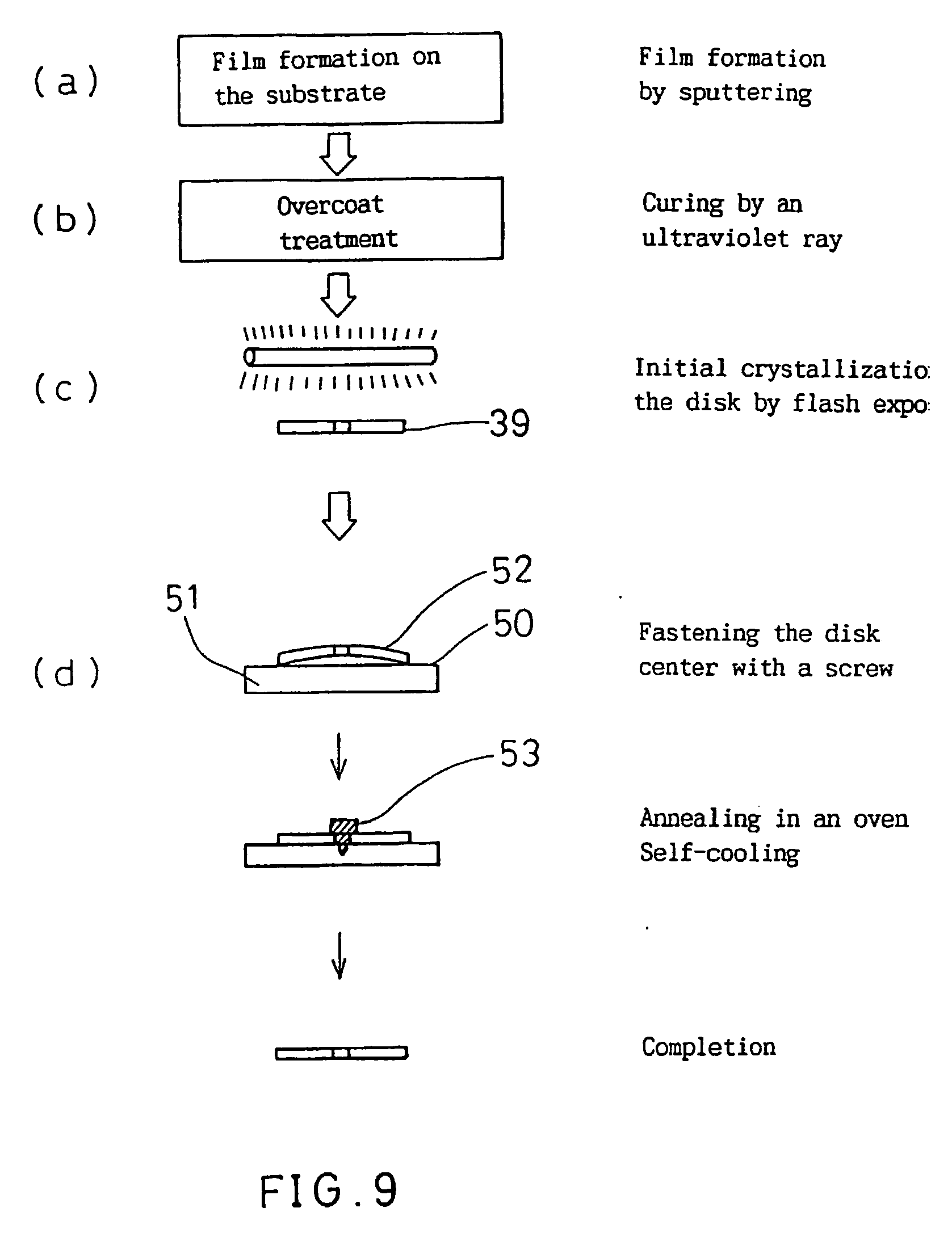
optical information recording materials with single side structure, in articular,
by applying an annealing process in combination with formation process of the resin
protection layer or a recording hin fil initialization process, the warp or distortion
of media caused by the contraction of the ultraviolet ray curing resin layer or the
recording thin film layer can be reduced or corrected to realize an optical information
recording medium having excellent servo characteristics. Further, by having at least
one of two media to be affixed with a transmissivity of an ultraviolet ray of 3 %
or more as a method to comprise an optical information recording medium with double
sides structure not liable to have a warp or distortion, an ultraviolet ray curing
resin can be used as an adhesive, resulting in simplifing the production process.
|
|
