(19)
(11) EP 2 180 514 A3

(12) EUROPEAN PATENT APPLICATION

(88) Date of publication A3:
23.03.2011 Bulletin 2011/12

(43) Date of publication A2:
28.04.2010 Bulletin 2010/17

(21) Application number: 09013174.9

(22) Date of filing: 19.10.2009
(51) International Patent Classification (IPC): 
H01L 27/146(2006.01)
H04N 5/335(2011.01)
H04N 3/15(0000.00)
(84) Designated Contracting States:
AT BE BG CH CY CZ DE DK EE ES FI FR GB GR HR HU IE IS IT LI LT LU LV MC MK MT NL NO PL PT RO SE SI SK SM TR
Designated Extension States:
AL BA RS

(30) Priority: 22.10.2008 JP 2008271673
29.05.2009 JP 2009129783
12.12.2008 JP 2008316452

(71) Applicant: Sony Corporation
Tokyo 108-0075 (JP)

(72) Inventors:
  • Yanagita, Takeshi
    Tokyo 108-0075 (JP)
  • Mabuchi, Keiji
    Tokyo 108-0075 (JP)
  • Ishiwata, Hiroaki
    Tokyo 108-0075 (JP)

(74) Representative: Müller - Hoffmann & Partner 
Patentanwälte Innere Wiener Strasse 17
81667 München
81667 München (DE)


(54) Solid state image sensor, method for driving a solid state image sensor, imaging apparatus, and electronic device


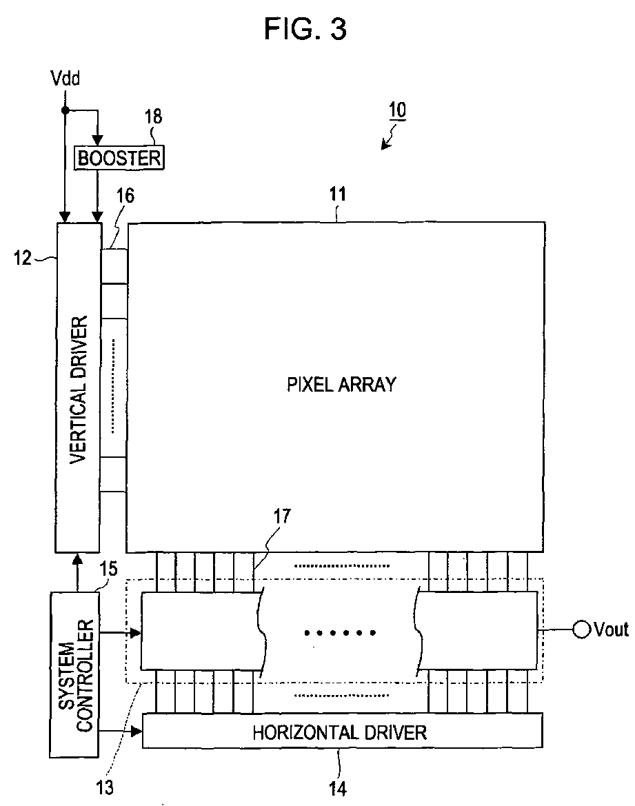
(57) A solid state image sensor includes a pixel array, as well as charge-to-voltage converters (FD1,FD2), reset gates (23), and amplifiers (24) each shared by a plurality of pixels in the array. The voltage level of the reset gate power supply (selecting power supply SELVdd) is set higher than the voltage level of the amplifier power supply (fixed power supply Vdd). Additionally, charge overflowing from photodetectors in the pixels may be discarded into the charge-to-voltage converters (FD1,FD2). The image sensor may also include a row scanner configured such that, while scanning a row in the pixel array to read out signals therefrom, the row scanner resets the charge in the photodetectors (21-1,21-2,21-3,21-4) of the pixels sharing a charge-to-voltage converter (FD1,FD2) with pixels on the readout row. The charge reset is conducted simultaneously with or prior to reading out the signals from the pixels on the readout row.


Search report