(19)
(11) EP 2 259 358 A3

(12) EUROPEAN PATENT APPLICATION

(88) Date of publication A3:
23.03.2011 Bulletin 2011/12

(43) Date of publication A2:
08.12.2010 Bulletin 2010/49

(21) Application number: 10164930.9

(22) Date of filing: 04.06.2010
(51) International Patent Classification (IPC): 
H01L 51/42(2006.01)
H01L 51/00(2006.01)
(84) Designated Contracting States:
AL AT BE BG CH CY CZ DE DK EE ES FI FR GB GR HR HU IE IS IT LI LT LU LV MC MK MT NL NO PL PT RO SE SI SK SM TR
Designated Extension States:
BA ME RS

(30) Priority: 03.06.2009 JP 2009134017
28.01.2010 JP 2010017477
03.06.2010 JP 2010127391

(71) Applicant: Fujifilm Corporation
Minato-ku Tokyo (JP)

(72) Inventors:
  • Mitsui, Tetsuro
    Kanagawa (JP)
  • Nomura, Kimiatsu
    Kanagawa (JP)
  • Yofu, Katsuyuki
    Kanagawa (JP)

(74) Representative: HOFFMANN EITLE 
Patent- und Rechtsanwälte Arabellastraße 4
81925 München
81925 München (DE)


(54) Photoelectric conversion device and imaging device


(57) Provided is a photoelectric conversion device comprising a transparent electrically conductive film, a photoelectric conversion film, and an electrically conductive film, wherein the photoelectric conversion film contains a compound represented by the following formula (i):

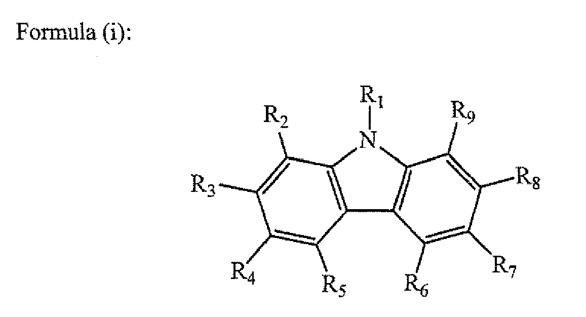
wherein each of R2 to R9 independently represents a hydrogen atom or a substituent, provided that each of at least two out of R3, R4, R7 and R8 independently represents an aryl group, a heterocyclic group or -N(Ra)(Rb), each of Ra and Rb independently represents a hydrogen atom or a substituent, and at least either Ra or Rb represents an aryl group or a heterocyclic group; and R1 represents an alkyl group, an aryl group or a heterocyclic group.


Search report