(19)
(11) EP 2 259 359 A3

(12) EUROPEAN PATENT APPLICATION

(88) Date of publication A3:
23.03.2011 Bulletin 2011/12

(43) Date of publication A2:
08.12.2010 Bulletin 2010/49

(21) Application number: 10164931.7

(22) Date of filing: 04.06.2010
(51) International Patent Classification (IPC): 
H01L 51/42(2006.01)
H01L 51/00(2006.01)
(84) Designated Contracting States:
AL AT BE BG CH CY CZ DE DK EE ES FI FR GB GR HR HU IE IS IT LI LT LU LV MC MK MT NL NO PL PT RO SE SI SK SM TR
Designated Extension States:
BA ME RS

(30) Priority: 05.06.2009 JP 2009136722
03.06.2010 JP 2010127490

(71) Applicant: Fujifilm Corporation
Minato-ku Tokyo (JP)

(72) Inventors:
  • Mitsui, Tetsuro
    Kanagawa (JP)
  • Nomura, Kimiatsu
    Kanagawa (JP)
  • Hamano, Mitsumasa
    Kanagawa (JP)

(74) Representative: HOFFMANN EITLE 
Patent- und Rechtsanwälte Arabellastraße 4
81925 München
81925 München (DE)


(54) Photoelectric conversion device, production method thereof and imaging device


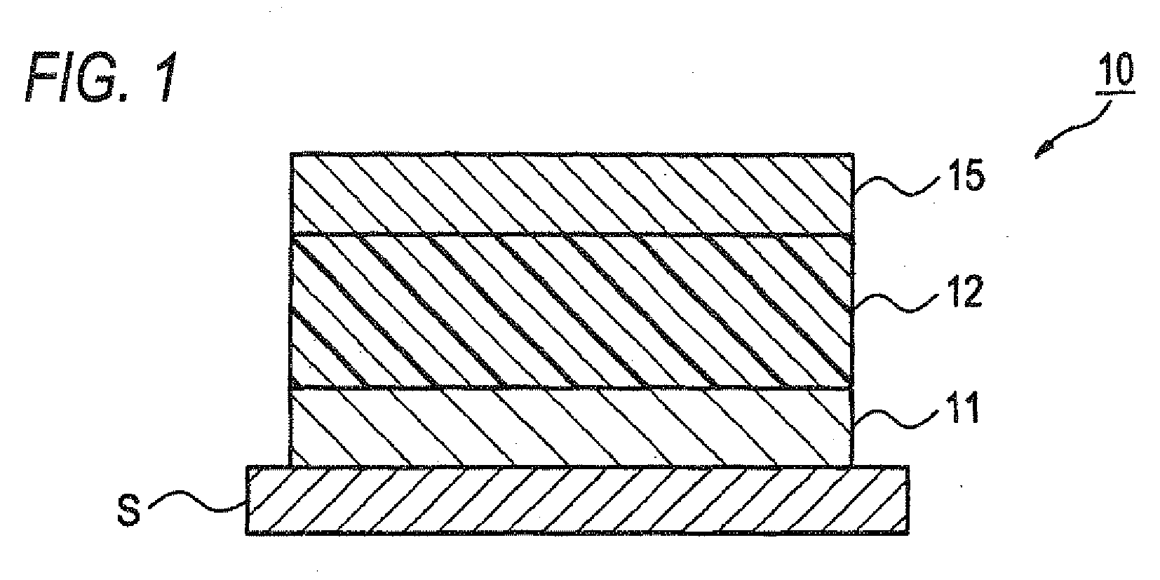
(57) Provided is a photoelectric conversion device comprising an electrically conductive film, a photoelectric conversion film, and a transparent electrically conductive film, wherein the photoelectric conversion film contains a fullerene or a fullerene derivative and a photoelectric conversion material having an absorption spectrum satisfying at least either the following condition (A) or (B):


wherein λL1, λL2, λM1 and λM2 are the wavelength at an absorption intensity of 1/2 of the maximum absorption intensity in the wavelength range of from 400 to 800 nm, each of λL1 and λL2 represents the wavelength in a chloroform solution spectrum when the photoelectric conversion material is dissolved in chloroform, and each of λM1 and λM2 represents the wavelength in a thin-film absorption spectrum of the photoelectric conversion material alone, provided that λL1L2 and λM1M2.


Search report