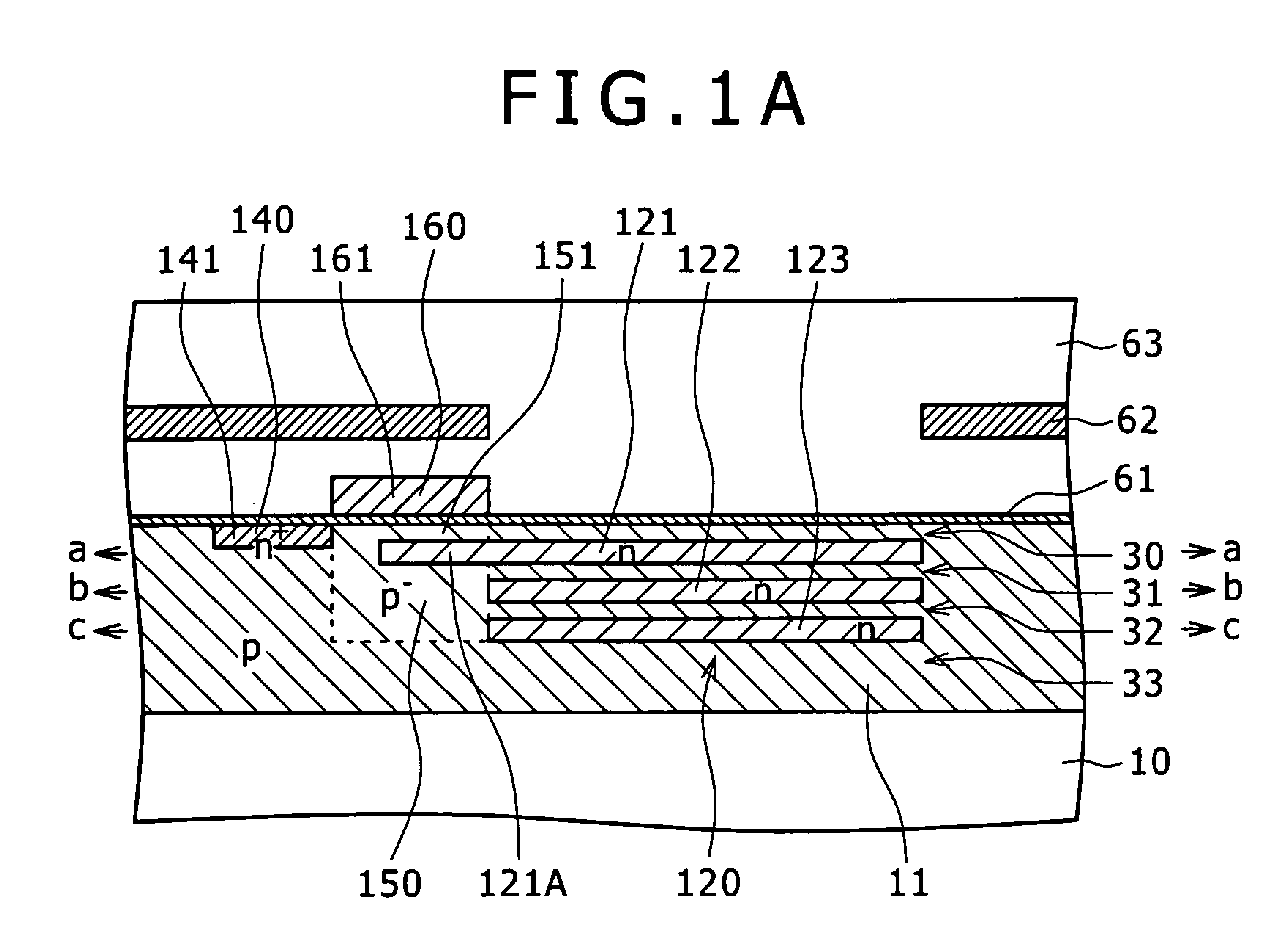
(57) A solid-state image pickup element includes: (A) a light receiving/charge accumulating
region (120) formed in a semiconductor layer (11) and formed by laminating M (where
M ≥ 2) light receiving/charge accumulating layers (121,122,123); (B) a charge outputting
region (140) formed in the semiconductor layer (11); (C) a depletion layer forming
region (150) formed of a part of the semiconductor layer (11), the part of the semiconductor
layer (11) being situated between the light receiving/charge accumulating region (120)
and the charge outputting region (140); and (D) a control electrode region (160) for
controlling a state of formation of a depletion layer in the depletion layer forming
region (150), wherein the solid-state image pickup element further includes light
receiving/charge accumulating layer extending section (121A,122A,123A) extending from
each light receiving/charge accumulating layer (121,122,123) to the depletion layer
forming region (150).
|
|
