|
(11) | EP 1 990 916 B1 |

| (12) | EUROPEAN PATENT SPECIFICATION |
|
|
| (54) |
Frequency modulator Frequenzmodulator Modulateur de fréquence |
|
|
|||||||||||||||||||||||||||||||
| Note: Within nine months from the publication of the mention of the grant of the European patent, any person may give notice to the European Patent Office of opposition to the European patent granted. Notice of opposition shall be filed in a written reasoned statement. It shall not be deemed to have been filed until the opposition fee has been paid. (Art. 99(1) European Patent Convention). |
[0001] The present invention relates to a frequency modulator, specifically a clock frequency modulator.
[0002] Devices adapted to modulate a clock frequency are known. A typical application for frequency modulators are switching regulators. A serious problem for switching regulators are in fact electromagnetic interferences (EMI) generated especially because of their fast switching features.
[0003] A possibility to reduce electromagnetic interferences consists in the periodic or random modulation of a parameter of the signals which are applied to switching devices, such as the switching frequency. The parameter oscillates with small amplitudes around a nominal value, so that the power of the harmonics is distributed on the spectrum. In order to reduce the emissions of electromagnetic interferences of the regulator and reduce the cost and size of the line filters, the switching frequency thereof needs to be modulated so that the resulting action on the distribution spectrum allows the distribution of the energy of each harmonic of the switching frequency on a number of sideband harmonics which have the same energy though a smaller amplitude.
[0004] A typical frequency modulator circuit adapted to generate a low-frequency triangular waveform is shown in Figure 1. The circuit includes a capacitor C which is connected to ground GND and to a current generator Ic connected to a supply voltage Vdd and to a switch S which may be connected to another current generator Icc connected to ground GND. The capacitor is also connected to the non-inverting terminal of a hysteresis comparator Comp having the inverting terminal connected to a reference voltage Vref. The output voltage of the comparator Comp controls the closing or opening of the switch S for the generation of a triangular wave on the non-inverting terminal of the comparator Comp. In order to modulate the frequency, the circuit topologies generally use the triangular waveform generated in this way as modulating reference voltage to control the oscillation frequency of the main oscillator.
[0005] In a completely integrated clock frequency modulator a low-frequency triangular wave needs to be generated without using external components. The triangular waveform is the modulating reference voltage which may be used to vary a circuit parameter of the oscillator so that the frequency of the oscillator is modulated by the modulating signal.
[0006] EP 1435694 discloses a spread spectrum clock generation circuit using a current control oscillator (ICO) wherein a differential signal to which a spread spectrum modulation signal, the period or amplitude of which changes is added, is generated, and the differential signal is applied to the ICO and a clock is generated. Such a spread spectrum clock generation circuit is capable of further reducing the electromagnetic wave radiation with a simple configuration.
[0007] US 2004/0213324 discloses a high frequency spread spectrum clock generation wherein, for EMI reduction, the current modulation profile is preferably used for frequencies over 1 GHz while the frequency deviation is increased at least to +-2.5 MHz and the modulation frequency is increased to at least 150 kHz, preferably about 260 kHz. In an alternative embodiment, the modification frequency is 1 MHz or greater so that a segmented spectrum is achieved. For clocks having basic frequency below 1 GHz, but having strong harmonics higher than 1 GHz, modulation of the foregoing is combined with the slower modulation currently used. EMI reduction is realized both at the lower and the higher harmonics.
[0008] In view of the state of the art a clock frequency modulator which is simpler than the known frequency modulators and which may be integrated needs to be provided.
[0009] According to the present invention it is provided an integrated circuit as defined in claim 1.
[0010] The features of the present invention will become apparent from the following detailed description of an embodiment thereof, shown by way of non-limiting example in the accompanying drawings, in which:
Figure 1 is a diagram of a clock frequency modulator according to the known art;
Figure 2 is a diagram of a clock frequency modulator according to an embodiment of the present invention;
Figure 3 shows a part of the modulator in Figure 2 in detail;
Figure 4 shows the time diagrams of signals involved in the modulator in figure 2;
Figure 5 shows the result of a simulation on the modulator in Figure 2.
[0011] Figure 2 shows a diagram of the frequency modulator according to the present invention. The diagram includes a digital-type triangular waveform generator 1, the output signal of which modulates an oscillator 2 adapted to provide the clock signal CLOCK.
[0012] The triangular waveform generator 1 is shown in greater detail in Figure 3. Said generator includes a first 3 and a second 4 frequency divider adapted to divide the frequency of the CLOCK signal by predetermined values which are different one from the other, a counter 5 supplied by the signals from the dividers 3 and 4 and a digital to analog converter (DAC) 6 having as an input the output signal from the counter 5 and adapted to generate the triangular waveform signal Vth.
[0013] Two signals are generated from the clock signal CLOCK; a high frequency signal CLKf generated by the divider 3 and a low frequency signal CLKb generated by the divider 4. The digital counter 5 is preferably an N-bit counter capable of increasingly and decreasingly counting. The signal CLKb, which has at least two logical levels, controls the counter 5 so that it increasingly or decreasingly counts while the signal CLKf is the counted signal; said signal is a pulse signal, which pulses are counted by the counter 5. The signal CLKb is generally a square wave signal and the counter 5 increasingly or decreasingly counts the pulses of the signal CLKf until the state of the signal CLKb changes; the counted digital word is issued in real time as an input to the DAC 6 which provides an output voltage value. The waveform of the modulating reference voltage signal Vth produced by the DAC 6 will be a triangular form.
[0014] The DAC has an input reference voltage signal Vstep and operates so that at each increase or decrease of the digital word counted by the counter 5 an increase or decrease of the voltage value Vstep of the voltage signal Vth is obtained; in this way the voltage signal Vth gains the waveform of a triangular wave signal of the type including voltage stepped ramps, each having the reference voltage value Vstep.
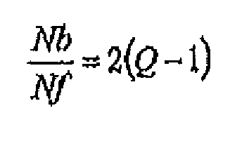
[0015] If Tb and Tf indicate the times associated with the frequencies of the signals CLKb and CLKf, the result is:
where Q indicates the number of quantisation levels; Tb=Nb/Fclock and Tf=Nf/Fclock is therefore obtained where Fclock indicates the frequency of the clock signal CLOCK and Nb and Nf are the ratios of the frequency dividers 4 and 3.
is therefore obtained.
[0016] The value of Q depends on the precision of the desired DAC and on the occupied area in the integrated circuit of the dividers 3 and 4. The same DAC 6 may have two input reference signals Vref1 and Vref2 instead of the voltage value Vstep, which reference signals Vref1 and Vref2 are adapted to respectively establish the minimum level and the maximum level of the modulating signal; the voltage value of the single step of the triangular waveform Vth of the stepped ramp type is obtained from the division of the difference between Vref2 and Vref1 and the value (Q-1).
[0017] In a specific application, the clock signal CLOCK is a 120 kHz square wave and is processed through the dividers 3 and 4 with Nb=504 and Nf=4 thus obtaining Q=64. The DAC 6 is a six-bit converter and produces a stepped triangular waveform by means of a voltage divider connected between two voltage reference values, a minimum voltage reference and a maximum voltage reference.
[0018] The mean value of the triangular wave 1,15 V is the voltage reference ensuring the fundamental frequency, whereas the amplitude value of about 80 mV determines the modulation depth of the clock frequency. The frequency of the triangular waveform is the lowest of the frequencies of the signal CLKb and it determines the modulating frequency. When Fclock=120 kHz and Nb=504, the modulating frequency is Fm=238 Hz.
1. An integrated circuit including an oscillator adapted to provide a clock frequency
and a clock frequency modulator of said clock frequency of the oscillator (2), said
oscillator generating a clock signal (CLOCK) at said clock frequency, said modulator
including digital means (1) for the generation of a signal (Vth) adapted to modulate
said clock frequency of the oscillator (2), said digital means (1) including first
means (3, 4) adapted to obtain from a clock signal (CLOCK) at its input a first pulse
signal (CLKf) having a lower frequency than the clock frequency of the oscillator,
a digital counter (5) adapted to count the pulses of said first signal (CLKf) and
to produce a digital signal and a digital to analog converter (6) adapted to convert
the digital signal in said signal (Vth) for modulating the clock frequency of the
oscillator, said first means (3, 4) being adapted to obtain from said clock signal
(CLOCK) generated by the oscillator a second signal (CLKb) having a lower frequency
than the frequency of the first signal (CLKf), said second signal assuming at least
two logical levels and said digital counter (5) being adapted to count up or down
the pulses of said first signal depending on the logical level of the second signal
characterised in that said clock signal at the input of said first means is the clock signal (CLOCK) generated
by said oscillator (2).
2. An integrated circuit according to claim 1, characterised in that said modulator includes a first (3) and a second (4) frequency divider of the clock
signal, said first divider (3) being adapted to divide the clock frequency by a first
amount (Nf) and said second divider (4) being adapted to divide the clock frequency
by a second amount (Nb) greater than the first amount (Nf), said first and second
dividers being adapted to respectively generate the first (CLKf) and the second (CLKb)
signal, said digital counter (5) being supplied by said first and second signals.
3. An integrated circuit according to claim 1, characterised in that said digital to analog converter (6) has at the input at least one reference voltage
(Vstep) and said digital signal, said digital to analog converter (6) being adapted
to generate said modulating signal with a triangular waveform (Vth), said triangular
waveform modulating signal including up and down step ramps, each step having the
absolute value of said reference signal.
4. An integrated circuit according to claim 2, characterised in that said digital to analog converter (6) has a first input reference voltage (Vref1)
adapted to establish the minimum level of the modulating signal and a second reference
voltage (Vref2) adapted to establish the maximum level of the modulating signal, said
digital to analog converter (6) being adapted to generate said triangular waveform
modulating signal (Vth) including up and down step ramps, each step having the value
obtained from the difference between said second (Vref2) and said first (Vref1) reference
voltages divided by a quantisation value Q decreased by one unit, said value Q being
obtained from the following equation:

where Nb indicates said second amount and Nf indicates said first amount.
where Nb indicates said second amount and Nf indicates said first amount.
1. Integrierte Schaltung, die einen Oszillator, der angepasst ist, eine Taktfrequenz
bereitzustellen, und einem Taktfrequenzmodulator für die Taktfrequenz des Oszillators
(2) aufweist, wobei der Oszillator ein Taktsignal (CLOCK) mit der Taktfrequenz erzeugt,
wobei der Modulator digitale Mittel (1) für die Erzeugung eines Signals (Vth) aufweist,
das angepasst ist, die Taktfrequenz des Oszillators (2) zu modulieren, wobei die digitalen
Mittel (1) aufweisen erste Mittel (3, 4), die angepasst sind, aus einem Taktsignal
(CLOCK) an deren Eingang ein erstes Pulssignal (CLKf) mit einer niedrigeren Frequenz
als die Taktfrequenz des Oszillators zu gewinnen, einen Digitalzähler (5), der angepasst
ist, die Pulse des ersten Signals (CLKf) zu zählen und ein Digitalsignal zu erzeugen,
und einen Digital-zu-Analog-Wandler (6), der angepasst ist, das Digitalsignal in das
Signal (Vth) zum Modulieren der Taktfrequenz des Oszillators zu wandeln, wobei die
ersten Mittel (3, 4), angepasst sind, aus dem Taktsignal (CLOCK), das durch den Oszillator
erzeugt wurde, ein zweites Signal (CLKb) mit einer niedrigeren Frequenz als die Frequenz
des ersten Signals (CLKf) zu gewinnen, wobei das zweite Signal wenigstens zwei Logikpegel
annimmt und der Digitalzähler (5) angepasst ist, die Pulse des ersten Signals abhängig
vorn dem Logikpegel des zweiten Signals auf oder abwärts zu zählen,
dadurch gekennzeichnet, dass das Taktsignal an dem Eingang der ersten Mittel das Taktsignal (CLOCK) ist, das durch den Oszillator (2) erzeugt wurde.
dadurch gekennzeichnet, dass das Taktsignal an dem Eingang der ersten Mittel das Taktsignal (CLOCK) ist, das durch den Oszillator (2) erzeugt wurde.
2. Integrierte Schaltung gemäß Anspruch 1, dadurch gekennzeichnet, dass der Modulator einen ersten (3) und einen zweiten (4) Frequenzteiler für das Taktsignal
aufweist, wobei der erste Teiler (3) angepasst ist, die Taktfrequenz durch einen ersten
Betrag (Nf) zu teilen, und der zweite Teiler (4) angepasst ist, die Taktfrequenz durch
einen zweiten Betrag (Nb), der größer als der erste Betrag (Nf) ist, zu teilen, wobei
der erste und der zweite Teiler angepasst sind, jeweils das erste (CLKf) und das zweite
(CLKb) Signal zu erzeugen, wobei der Digitalzähler (5) mit dem ersten und dem zweiten
Signal gespeist wird.
3. Integrierte Schaltung gemäß Anspruch 1, dadurch gekennzeichnet, dass der Digital-zu-Analog-Wandler (6) an dem Eingang wenigstens eine Referenzspannung
(Vstep) und das Digitalsignal aufweist, wobei der Digital-zu-Analog-Wandler (6) angepasst
ist, das Modulationssignal mit einer Dreieckswellenform (Vth) zu erzeugen, wobei das
Dreieckswellenform-Modulationssignal Aufwärts- und Abwärtsstufenrampen aufweist, wobei
jede Stufe den Absolutwert des Referenzsignals aufweist.
4. Integrierte Schaltung gemäß Anspruch 2, dadurch gekennzeichnet, dass der Digital-zu-Analog-Wandler (6) eine erste Eingangsreferenzspannung (Vref1) aufweist,
die angepasst ist, den Minimalpegel des Modulationssignals fest zu legen und eine
zweite Referenzspannung (Vref2), die angepasst ist, den Maximalpegel des Modulationssignals
fest zu legen, wobei der Digital-zu-Analog-Wandler (6) angepasst ist, das Dreieckswellenform-Modulationssignal
(Vth) mit Aufwärts- und Abwärtsstufenrampen zu erzeugen, wobei jede Stufe einen Wert
aufweist, der aus der Differenz zwischen der zweiten (Vref2) und der ersten (Vref1)
Referenzspannungen geteilt durch einen um eins verringerten Quantisierungswert Q geteilt
wird, wobei der Wert Q aus der folgenden Gleichung erhalten wird:
wobei Nb den zweiten Betrag und Nf den ersten Betrag anzeigt.
wobei Nb den zweiten Betrag und Nf den ersten Betrag anzeigt.
1. Circuit intégré comprenant un oscillateur adapté pour fournir une fréquence d'horloge
et un modulateur de fréquence d'horloge de ladite fréquence d'horloge de l'oscillateur
(2), ledit oscillateur générant un signal d'horloge (CLOCK) à ladite fréquence d'horloge,
ledit modulateur comprenant un moyen numérique (1) pour la génération d'un signal
(Vth) adapté pour moduler ladite fréquence d'horloge de l'oscillateur (2), ledit moyen
numérique (1) comprenant un premier moyen (3, 4) adapté pour obtenir d'un signal d'horloge
(CLOCK) appliqué à son entrée un premier signal d'impulsion (CLKf) ayant une fréquence
inférieure à la fréquence d'horloge de l'oscillateur, un compteur numérique (5) adapté
pour compter les impulsions dudit premier signal (CLKf) et pour produire un signal
numérique et un convertisseur numérique-analogique (6) adapté pour convertir le signal
numérique en ledit signal (Vth) pour moduler la fréquence d'horloge de l'oscillateur,
ledit premier moyen (3, 4) étant adapté pour obtenir dudit signal d'horloge (CLOCK)
généré par l'oscillateur un deuxième signal (CLKb) ayant une fréquence inférieure
à la fréquence du premier signal (CLKf), ledit deuxième signal prenant au moins deux
niveaux logiques et ledit compteur numérique (5) étant adapté pour compter de façon
croissante ou décroissante les impulsions dudit premier signal en fonction du niveau
logique du deuxième signal ;
caractérisé en ce que ledit signal d'horloge en entrée dudit premier moyen est le signal d'horloge (CLOCK) généré par ledit oscillateur (2).
caractérisé en ce que ledit signal d'horloge en entrée dudit premier moyen est le signal d'horloge (CLOCK) généré par ledit oscillateur (2).
2. Circuit intégré selon la revendication 1, caractérisé en ce que ledit modulateur comprend un premier (3) et un deuxième (4) diviseur de fréquence
du signal d'horloge, ledit premier diviseur (3) étant adapté pour diviser la fréquence
d'horloge d'une première valeur (Nf) et ledit deuxième diviseur (4) étant adapté pour
diviser la fréquence d'horloge d'une deuxième valeur (Nb) supérieure à la première
valeur (Nf), lesdits premier et deuxième diviseurs étant adaptés pour générer respectivement
le premier signal (CLKf) et le deuxième signal (CLKb), ledit compteur numérique (5)
étant fourni par lesdits premier et deuxième signaux.
3. Circuit intégré selon la revendication 1, caractérisé en ce que ledit convertisseur numérique-analogique (6) a en entrée au moins une tension de
référence (Vstep) et ledit signal numérique, ledit convertisseur numérique-analogique
(6) étant adapté pour générer ledit signal de modulation avec une forme d'onde triangulaire
(Vth), ledit signal de modulation à forme d'onde triangulaire comprenant des rampes
étagées montantes et descendantes, chaque étage ayant la valeur absolue dudit signal
de référence.
4. Circuit intégré selon la revendication 2, caractérisé en ce que ledit convertisseur numérique-analogique (6) a une première tension de référence
d'entrée (Vref1) adaptée pour établir le niveau minimum du signal de modulation et
une deuxième tension de référence (Vref2) adaptée pour établir le niveau maximum du
signal de modulation, ledit convertisseur numérique-analogique (6) étant adapté pour
générer ledit signal de modulation à forme d'onde triangulaire (Vth) comprenant des
rampes étagées montantes et descendantes, chaque étage ayant la valeur obtenue à partir
de la différence entre ladite deuxième tension de référence (Vref2) et ladite première
tension de référence (Vref1) divisée par une valeur de quantification Q diminuée d'une
unité, ladite valeur Q étant obtenue au moyen de l'équation suivante :

où Nb représente ladite deuxième valeur et Nf représente ladite première valeur.
où Nb représente ladite deuxième valeur et Nf représente ladite première valeur.
REFERENCES CITED IN THE DESCRIPTION
This list of references cited by the applicant is for the reader's convenience only. It does not form part of the European patent document. Even though great care has been taken in compiling the references, errors or omissions cannot be excluded and the EPO disclaims all liability in this regard.
Patent documents cited in the description