(19)
(11) EP 2 669 938 A3

(12) EUROPEAN PATENT APPLICATION

(88) Date of publication A3:
09.04.2014 Bulletin 2014/15

(43) Date of publication A2:
04.12.2013 Bulletin 2013/49

(21) Application number: 13169401.0

(22) Date of filing: 27.05.2013
(51) International Patent Classification (IPC): 
H01L 21/60(2006.01)
H01L 23/544(2006.01)
H01L 25/07(2006.01)
H01L 23/373(2006.01)
H01L 21/48(2006.01)
(84) Designated Contracting States:
AL AT BE BG CH CY CZ DE DK EE ES FI FR GB GR HR HU IE IS IT LI LT LU LV MC MK MT NL NO PL PT RO RS SE SI SK SM TR
Designated Extension States:
BA ME

(30) Priority: 28.05.2012 JP 2012120376

(71) Applicant: Hitachi Ltd.
Tokyo 100-8280 (JP)

(72) Inventors:
  • Kumagai, Yukihiro
    Tokyo 100-8220 (JP)
  • Hiyoshi, Michiaki
    Tokyo 100-8220 (JP)

(74) Representative: Beetz & Partner 
Patentanwälte Steinsdorfstraße 10
80538 München
80538 München (DE)


(54) Semiconductor device with an oxide solder flow prevention area on a substrate and corresponding manufacturing method


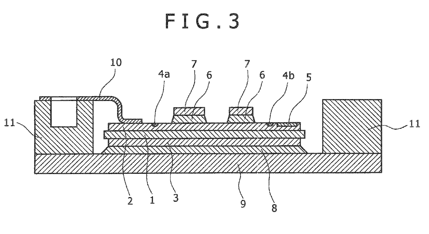
(57) In a semiconductor device where a metal circuit layer (2) is disposed over a main planar surface of an insulating substrate (1), a semiconductor chip (7) is connected by way of a solder (6) to the metal circuit layer (2), and a metal terminal (10) is ultrasonically connected to the metal circuit layer (2), in which a solder flow prevention area (4a, 4b, 12a, 12b) comprising an oxide material is linearly formed between the semiconductor chip (7) and the ultrasonic metal bonding region (53) over the metal circuit layer (2). The oxide solder flow prevention area (4a, 4b, 12a, 12b) may be formed by local laser irradiation of the metal circuit layer (2). A mark (5) may be formed to the metal circuit layer (2), using an identical laser irradiation device.


Search report


Search report