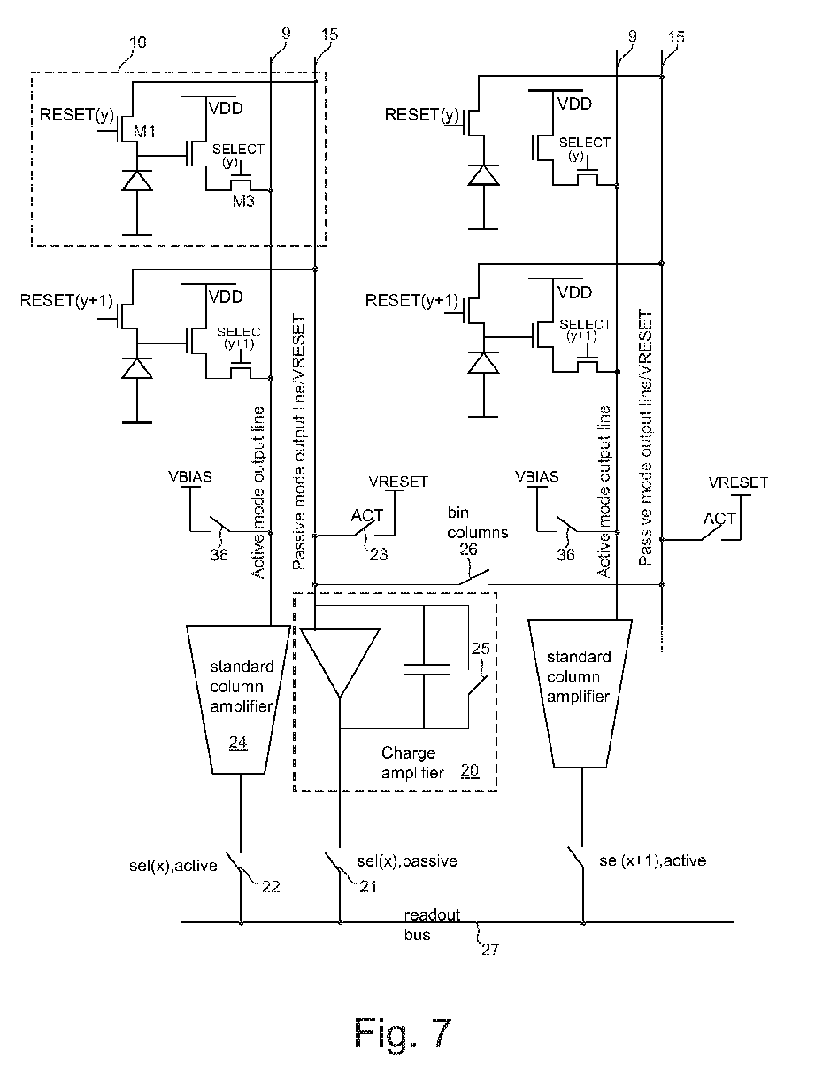
(57) A pixel array comprises pixels (10) arranged in columns. A pixel (10) comprises a
photo-sensitive element (11) for generating charges responsive to electromagnetic
radiation and a buffer amplifier (M2) for buffering a voltage proportional to the
charges generated by the photo-sensitive element. A first switch (M3) selectively
connects an output of the buffer amplifier to an active pixel mode column output line
(9). A second switch (M1) selectively transfers at least part of the charges generated
by the photo-sensitive element (11) to a passive pixel mode column output line (15).
The pixel (10) can be selectively operated in a conventional, active pixel mode, and
in a passive pixel/charge binning mode. The second switch (M1) can be a reset switch,
with the second output line operable, on a time-shared basis, as a supply line for
providing the reference voltage. Another embodiment has the first switch and the second
switch connected to a single column output line which is operable, on a time-shared
basis, as the active pixel mode column output line and as the passive pixel mode column
output line.
|
|
