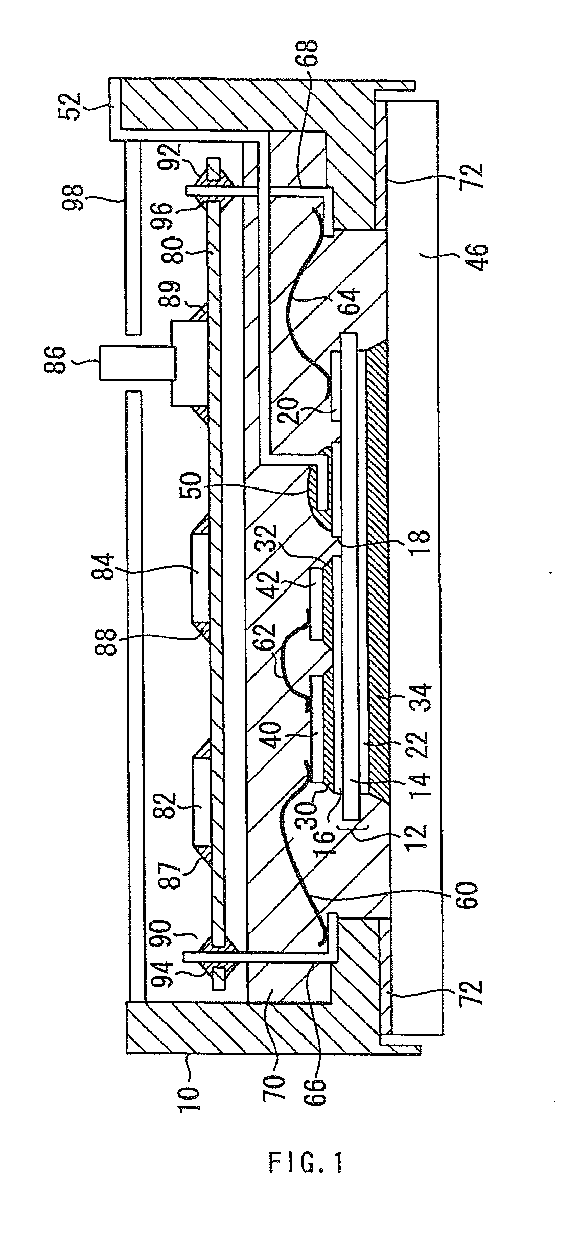
(57) A power semiconductor device includes a substrate (14), an element circuit pattern
(16) formed on the substrate (14) and made of Cu optionally covered with an electroless-plated
Ni-P layer, and a power semiconductor element (40,42) bonded to the element circuit
pattern (16) by a solder (30,32), wherein the solder (30,32) is an alloy of Sn, Sb,
and Cu, the Sb content being in the range of 6.5 to 8 weight % and the Cu content
being in the range of 0.5 to 1 weight %. A terminal (52) is bonded to a terminal circuit
pattern (18, 20) formed on the substrate (14) by a terminal solder (50) made of a
Sn-Ag-based or Sn-Ag-Cu-based unleaded solder. A heat sink (46) is bonded to a surface
pattern (22) formed on the bottom surface the substrate (14) by a solder (34) having
the same composition as the Sn-Sb-Cu solder (30, 32).
|
|
