(19)
(11) EP 2 355 177 A3

(12) EUROPEAN PATENT APPLICATION

(88) Date of publication A3:
10.12.2014 Bulletin 2014/50

(43) Date of publication A2:
10.08.2011 Bulletin 2011/32

(21) Application number: 11151792.6

(22) Date of filing: 24.01.2011
(51) International Patent Classification (IPC): 
H01L 33/00(2010.01)
H01L 33/38(2010.01)
H01L 33/20(2010.01)
H01L 25/16(2006.01)
(84) Designated Contracting States:
AL AT BE BG CH CY CZ DE DK EE ES FI FR GB GR HR HU IE IS IT LI LT LU LV MC MK MT NL NO PL PT RO RS SE SI SK SM TR
Designated Extension States:
BA ME

(30) Priority: 04.02.2010 KR 20100010246

(71) Applicant: LG Innotek Co., Ltd.
Seoul 100-714 (KR)

(72) Inventor:
  • Jeong, Hwan Hee
    100-714 Seoul (KR)

(74) Representative: Cabinet Plasseraud 
52, rue de la Victoire
75440 Paris Cedex 09
75440 Paris Cedex 09 (FR)


(54) Light emitting device, method of manufacturing the same


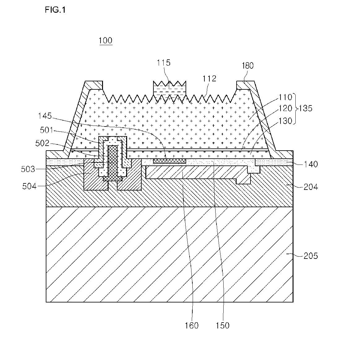
(57) Disclosed are a light emitting device, a method of manufacturing the same, a light emitting device package, and a lighting system. The light emitting device includes the light emitting structure layer including a first conductive semiconductor layer (110), a second conductive semiconductor layer (130), and an active layer (120) between the first and second conductive semiconductor layers, a conductive support substrate (205) electrically connected to the second conductive semiconductor layer, a contact (502) electrically connected to the first conductive semiconductor layer, a dielectric material (503) making contact with the contact and interposed between the contact and the conductive support substrate, and an insulating layer (501,504) electrically insulating the contact from the active layer, the second conductive semiconductor layer, and the conductive support substrate.


Search report


Search report